SBAS980B June   2019  – June 2020 TLA2518

PRODUCTION DATA.  

  1. Features
  2. Applications
  3. Description
    1.     Device Images
      1.      TLA2518 Block Diagram and Applications
  4. Revision History
  5. Pin Configuration and Functions
    1.     Pin Functions
  6. Specifications
    1. 6.1 Absolute Maximum Ratings
    2. 6.2 ESD Ratings
    3. 6.3 Recommended Operating Conditions
    4. 6.4 Thermal Information
    5. 6.5 Electrical Characteristics
    6. 6.6 Timing Requirements
    7. 6.7 Switching Characteristics
    8. 6.8 Typical Characteristics
  7. Detailed Description
    1. 7.1 Overview
    2. 7.2 Functional Block Diagram
    3. 7.3 Feature Description
      1. 7.3.1 Multiplexer and ADC
      2. 7.3.2 Reference
      3. 7.3.3 ADC Transfer Function
      4. 7.3.4 ADC Offset Calibration
      5. 7.3.5 Programmable Averaging Filter
      6. 7.3.6 General-Purpose I/Os
      7. 7.3.7 Oscillator and Timing Control
      8. 7.3.8 Output Data Format
      9. 7.3.9 Device Programming
        1. 7.3.9.1 Enhanced-SPI Interface
        2. 7.3.9.2 Register Read/Write Operation
          1. 7.3.9.2.1 Register Write
          2. 7.3.9.2.2 Register Read
    4. 7.4 Device Functional Modes
      1. 7.4.1 Device Power-Up and Reset
      2. 7.4.2 Manual Mode
      3. 7.4.3 On-the-Fly Mode
      4. 7.4.4 Auto-Sequence Mode
    5. 7.5 TLA2518 Registers
      1. 7.5.1  SYSTEM_STATUS Register (Address = 0x0) [reset = 0x81]
        1. Table 9. SYSTEM_STATUS Register Field Descriptions
      2. 7.5.2  GENERAL_CFG Register (Address = 0x1) [reset = 0x0]
        1. Table 10. GENERAL_CFG Register Field Descriptions
      3. 7.5.3  DATA_CFG Register (Address = 0x2) [reset = 0x0]
        1. Table 11. DATA_CFG Register Field Descriptions
      4. 7.5.4  OSR_CFG Register (Address = 0x3) [reset = 0x0]
        1. Table 12. OSR_CFG Register Field Descriptions
      5. 7.5.5  OPMODE_CFG Register (Address = 0x4) [reset = 0x0]
        1. Table 13. OPMODE_CFG Register Field Descriptions
      6. 7.5.6  PIN_CFG Register (Address = 0x5) [reset = 0x0]
        1. Table 14. PIN_CFG Register Field Descriptions
      7. 7.5.7  GPIO_CFG Register (Address = 0x7) [reset = 0x0]
        1. Table 15. GPIO_CFG Register Field Descriptions
      8. 7.5.8  GPO_DRIVE_CFG Register (Address = 0x9) [reset = 0x0]
        1. Table 16. GPO_DRIVE_CFG Register Field Descriptions
      9. 7.5.9  GPO_VALUE Register (Address = 0xB) [reset = 0x0]
        1. Table 17. GPO_VALUE Register Field Descriptions
      10. 7.5.10 GPI_VALUE Register (Address = 0xD) [reset = 0x0]
        1. Table 18. GPI_VALUE Register Field Descriptions
      11. 7.5.11 SEQUENCE_CFG Register (Address = 0x10) [reset = 0x0]
        1. Table 19. SEQUENCE_CFG Register Field Descriptions
      12. 7.5.12 CHANNEL_SEL Register (Address = 0x11) [reset = 0x0]
        1. Table 20. CHANNEL_SEL Register Field Descriptions
      13. 7.5.13 AUTO_SEQ_CH_SEL Register (Address = 0x12) [reset = 0x0]
        1. Table 21. AUTO_SEQ_CH_SEL Register Field Descriptions
  8. Application and Implementation
    1. 8.1 Application Information
    2. 8.2 Typical Applications
      1. 8.2.1 Mixed-Channel Configuration
        1. 8.2.1.1 Design Requirements
        2. 8.2.1.2 Detailed Design Procedure
          1. 8.2.1.2.1 Digital Input
          2. 8.2.1.2.2 Digital Open-Drain Output
        3. 8.2.1.3 Application Curve
      2. 8.2.2 Digital Push-Pull Output Configuration
  9. Power Supply Recommendations
    1. 9.1 AVDD and DVDD Supply Recommendations
  10. 10Layout
    1. 10.1 Layout Guidelines
    2. 10.2 Layout Example
  11. 11Device and Documentation Support
    1. 11.1 Receiving Notification of Documentation Updates
    2. 11.2 Support Resources
    3. 11.3 Trademarks
    4. 11.4 Electrostatic Discharge Caution
    5. 11.5 Glossary
  12. 12Mechanical, Packaging, and Orderable Information

Package Options

Mechanical Data (Package|Pins)
Thermal pad, mechanical data (Package|Pins)
Orderable Information

On-the-Fly Mode

In the on-the-fly mode of operation, the analog input channel is selected, as shown in Figure 32, using the first five bits on SDI without waiting for the CS rising edge. Thus, the ADC samples the newly selected channel on the CS edge and there is no latency between the channel selection and the ADC output data.
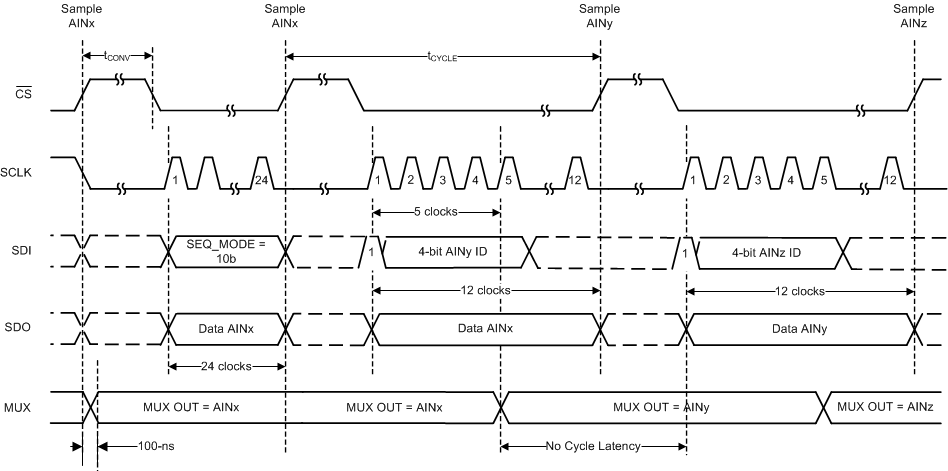
TLA2518 on-the-fly_mode.gifFigure 32. Starting Conversions and Reading Data in On-the-Fly Mode

The number of clocks required for reading the output data depends on the device output data frame size; see the Output Data Format section for more details.