SLOS154C December 1995 – July 2025 TLC27L1 , TLC27L1A
PRODUCTION DATA
- 1
- 1 Features
- 2 Applications
- 3 Description
- 4 Pin Configuration and Functions
-
5 Specifications
- 5.1 Absolute Maximum Ratings
- 5.2 Dissipation Ratings
- 5.3 Recommended Operating Conditions
- 5.4 Electrical Characteristics, C Suffix
- 5.5 Operating Characteristics, VDD = 5V, C Suffix
- 5.6 Operating Characteristics, VDD = 10V, C Suffix
- 5.7 Electrical Characteristics, I Suffix
- 5.8 Operating Characteristics, VDD = 5V, I Suffix
- 5.9 Operating Characteristics, VDD = 10V, I Suffix
- 5.10 Typical Characteristics
- 6 Parameter Measurement Information
- 7 Application and Implementation
- 8 Device and Documentation Support
- 9 Revision History
- 10Mechanical, Packaging, and Orderable Information
Package Options
Refer to the PDF data sheet for device specific package drawings
Mechanical Data (Package|Pins)
- D|8
Thermal pad, mechanical data (Package|Pins)
Orderable Information
4 Pin Configuration and Functions
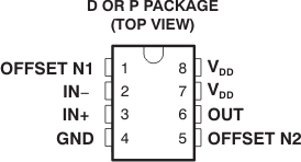
 Figure 4-1 D Package,8-Pin SOIC, or P Package, 8-Pin PDIP (Top View)
Table 4-1 Pin Functions
| PIN | TYPE | DESCRIPTION | |
|---|---|---|---|
| NAME | NO. | ||
| GND | 4 | Ground | Ground or negative (lowest) power supply |
| IN+ | 3 | Input | Noninverting input |
| IN– | 2 | Input | Inverting input |
| OFFSET N1 | 1 | Input | On legacy silicon: IN– offset adjustment pin (bias-select). On new silicon: NC, non internally connected pin |
| OFFSET N2 | 5 | Input | On legacy silicon: IN+ offset adjustment pin (bias-select). On new silicon: NC, non internally connected pin |
| OUT | 6 | Output | Output |
| VDD | 7, 8 | Power | Positive (highest) power supply |