SLVSCO9A August 2015 – August 2015 TLC6C5712-Q1
PRODUCTION DATA.
- 1 Features
- 2 Applications
- 3 Description
- 4 Revision History
- 5 Pin Configuration and Functions
- 6 Specifications
-
7 Detailed Description
- 7.1 Overview
- 7.2 Functional Block Diagram
- 7.3
Feature Description
- 7.3.1 Power-On Reset (POR)
- 7.3.2 Error Feedback
- 7.3.3 PWM Input
- 7.3.4 Constant-Current Output
- 7.3.5 Advanced Diagnostics
- 7.3.6 Register Protection
- 7.3.7 Serial Interface - SPI
- 7.3.8 Thermal Information
- 7.4 Device Functional Modes
- 7.5
Register Maps
- 7.5.1 WRITE_MAP0 Register (address = 40h) [reset = 00h]
- 7.5.2 WRITE_MAP1 Register (address = 41h) [reset = 00h]
- 7.5.3 WRITE_MAP2 Register (address = 42h) [reset = 00h]
- 7.5.4 WRITE_MAP3 Register (address = 43h) [reset = 00h]
- 7.5.5 WRITE_MAP4 Register (address = 44h) [reset = 00h]
- 7.5.6 WRITE_MAP5 Register (address = 45h) [reset = 00h]
- 7.5.7 WRITE_CORR0 Register (address = 46h) [reset = 00h]
- 7.5.8 WRITE_CORR1 Register (address = 47h) [reset = 00h]
- 7.5.9 WRITE_CORR2 Register (address = 48h) [reset = 00h]
- 7.5.10 WRITE_CORR3 Register (address = 49h) [reset = 00h]
- 7.5.11 WRITE_CORR4 Register (address = 4Ah) [reset = 00h]
- 7.5.12 WRITE_CORR5 Register (address = 4Bh) [reset = 00h]
- 7.5.13 WRITE_CORR6 Register (address = 4Ch) [reset = 00h]
- 7.5.14 WRITE_CORR7 Register (address = 4Dh) [reset = 00h]
- 7.5.15 WRITE_CORR8 Register (address = 4Eh) [reset = 00h]
- 7.5.16 WRITE_CORR9 Register (address = 4Fh) [reset = 00h]
- 7.5.17 WRITE_CORR10 Register (address = 50h) [reset = 00h]
- 7.5.18 WRITE_CORR11 Register (address = 51h) [reset = 00h]
- 7.5.19 WRITE_CH_ON_MASK0 Register (address = 52h) [reset = 3Fh]
- 7.5.20 WRITE_CH_ON_MASK1 Register (address = 53h) [reset = 3Fh]
- 7.5.21 WRITE_SHORT_MASK0 Register (address = 54h) [reset = 3Fh]
- 7.5.22 WRITE_SHORT_MASK1 Register (address = 55h) [reset = 3Fh]
- 7.5.23 WRITE_SHORT_GND_MASK0 Register (address = 56h) [reset = 3Fh]
- 7.5.24 WRITE_SHORT_GND_MASK1 Register (address = 57h) [reset = 3Fh]
- 7.5.25 WRITE_OPEN_MASK0 Register (address = 58h) [reset = 3Fh]
- 7.5.26 WRITE_OPEN_MASK1 Register (address = 59h) [reset = 3Fh]
- 7.5.27 WRITE_PWM_FAULT_MASK Register (address = 60h) [reset = 3Fh]
- 7.5.28 RESET_POR Register (address = 61h) [reset = 00h]
- 7.5.29 RESET_STATUS Register (address = 62h) [reset = 00h]
- 7.5.30 SOFTWARE_POR Register (address = 63h) [reset = 00h]
- 7.5.31 WRITE_DIS_PULL_UP_0 Register (address = 64h) [reset = 00h]
- 7.5.32 WRITE_DIS_PULL_UP_1 Register (address = 65h) [reset = 00h]
- 7.5.33 WRITE_ERROR_MASK Register (address = 66h) [reset = 00h]
- 7.5.34 WRITE_MISC_CMD Register (address = 67h) [reset = 00h]
- 7.5.35 LOCK_MAP Register (address = 68h) [reset = 00h]
- 7.5.36 LOCK_CORR Register (address = 69h) [reset = 00h]
- 7.5.37 LOCK_MASK Register (address = 6Ah) [reset = 00h]
- 7.5.38 LOCK_MISC Register (address = 6Bh) [reset = 00h]
- 7.5.39 UNLOCK_MAP Register (address = 6Ch) [reset = 00h]
- 7.5.40 UNLOCK_CORR Register (address = 6Dh) [reset = 00h]
- 7.5.41 UNLOCK_MASK Register (address = 6Eh) [reset = 00h]
- 7.5.42 UNLOCK_MISC Register (address = 6Fh) [reset = 00h]
- 7.5.43 READ_MAP0 Register (address = 80h) [reset = 00h]
- 7.5.44 READ_MAP1 Register (address = 81h) [reset = 00h]
- 7.5.45 READ_MAP2 Register (address = 82h) [reset = 00h]
- 7.5.46 READ_MAP3 Register (address = 83h) [reset = 00h]
- 7.5.47 READ_MAP4 Register (address = 84h) [reset = 00h]
- 7.5.48 READ_MAP5 Register (address = 85h) [reset = 00h]
- 7.5.49 READ_CORR0 Register (address = 86h) [reset = 00h]
- 7.5.50 READ_CORR1 Register (address = 87h) [reset = 00h]
- 7.5.51 READ_CORR2 Register (address = 88h) [reset = 00h]
- 7.5.52 READ_CORR3 Register (address = 89h) [reset = 00h]
- 7.5.53 READ_CORR4 Register (address = 8Ah) [reset = 00h]
- 7.5.54 READ_CORR5 Register (address = 8Bh) [reset = 00h]
- 7.5.55 READ_CORR6 Register (address = 8Ch) [reset = 00h]
- 7.5.56 READ_CORR7 Register (address = 8Dh) [reset = 00h]
- 7.5.57 READ_CORR8 Register (address = 8Eh) [reset = 00h]
- 7.5.58 READ_CORR9 Register (address = 8Fh) [reset = 00h]
- 7.5.59 READ_CORR10 Register (address = 90h) [reset = 00h]
- 7.5.60 READ_CORR11 Register (address = 91h) [reset = 00h]
- 7.5.61 READ_CH_ON_MASK0 Register (address = 92h) [reset = 3Fh]
- 7.5.62 READ_CH_ON_MASK1 Register (address = 93h) [reset = 3Fh]
- 7.5.63 READ_SHORT_MASK0 Register (address = 94h) [reset = 3Fh]
- 7.5.64 READ_SHORT_MASK1 Register (address = 95h) [reset = 3Fh]
- 7.5.65 READ_SHORT_GND_MASK0 Register (address = 96h) [reset = 3Fh]
- 7.5.66 READ_SHORT_GND_MASK1 Register (address = 97h) [reset = 3Fh]
- 7.5.67 READ_OPEN_MASK0 Register (address = 98h) [reset = 3Fh]
- 7.5.68 READ_OPEN_MASK1 Register (address = 99h) [reset = 3Fh]
- 7.5.69 READ_SHORT_FAULT0 (address = 9Ah) [reset = 00h]
- 7.5.70 READ_SHORT_FAULT1 (address = 9Bh) [reset = 00h]
- 7.5.71 READ_SHORT_GND_FAULT0 (address = 9Ch) [reset = 00h]
- 7.5.72 READ_SHORT_GND_FAULT1 (address = 9Dh) [reset = 00h]
- 7.5.73 READ_OPEN_FAULT0 (address = 9Eh) [reset = 00h]
- 7.5.74 READ_OPEN_FAULT1 (address = 9Fh) [reset = 00h]
- 7.5.75 READ_PWM_FAULT_MASK Register (address = A1h) [reset = 3Fh]
- 7.5.76 READ_STATUS0 (address = A2h) [reset = 40h]
- 7.5.77 READ_STATUS1 (address = A3h) [reset = 00h]
- 7.5.78 READ_DIS_PULL_UP_0 Register (address = A4h) [reset = 00h]
- 7.5.79 READ_DIS_PULL_UP_1 Register (address = A5h) [reset = 00h]
- 7.5.80 READ_ERROR_MASK (address = A6h) [reset = 00h]
- 7.5.81 READ_MISC_CMD Register (address = A7h) [reset = 00h]
- 7.5.82 READ_ADSHORT0 (address = A8h) [reset = 00h]
- 7.5.83 READ_ADSHORT1 (address = A9h) [reset = 00h]
- 8 Application and Implementation
- 9 Power Supply Recommendations
- 10Layout
- 11Device and Documentation Support
- 12Mechanical, Packaging, and Orderable Information
Package Options
Mechanical Data (Package|Pins)
- PWP|28
Thermal pad, mechanical data (Package|Pins)
- PWP|28
Orderable Information
6 Specifications
6.1 Absolute Maximum Ratings
over operating ambient temperature range. Voltages referenced with respect to GND (unless otherwise noted)(1)(2)| MIN | MAX | UNIT | ||
|---|---|---|---|---|
| Input voltage | VCC | –0.3 | 7 | V |
| IREF, LATCH, PWMx, SCK, SDI | –0.3 | VCC | ||
| SENSE | –0.3 | 10 | ||
| Output voltage | ERR open-drain output | –0.3 | 7 | V |
| OUTx power DMOS drain-to-source voltage | –0.3 | 10 | ||
| SDO | –0.3 | VCC | ||
| Ground | PGND | –0.3 | 0.3 | V |
| Operating ambient temperature, TA | –40 | 125 | °C | |
| Operating junction temperature, TJ | –40 | 150 | °C | |
| Storage temperature range, Tstg | –55 | 150 | °C | |
(1) Stresses beyond those listed under Absolute Maximum Ratings may cause permanent damage to the device. These are stress ratings only, which do not imply functional operation of the device at these or any other conditions beyond those indicated under Recommended Operating Conditions. Exposure to absolute-maximum-rated conditions for extended periods may affect device reliability.
(2) All voltages are measured relative to GND.
6.2 ESD Ratings
| VALUE | UNIT | ||||
|---|---|---|---|---|---|
| V(ESD) | Electrostatic discharge | Human body model (HBM), per AEC Q100-002(1) | ±2000 | V | |
| Charged device model (CDM), per AEC Q100-011 | All pins | ±500 | V | ||
| Corner pins (1, 14, 15, and 28) | ±750 | ||||
(1) AEC Q100-002 indicates HBM stressing shall be in accordance with the ANSI/ESDA/JEDEC JS-001 specification.
6.3 Recommended Operating Conditions
over operating free-air temperature range (unless otherwise noted)| MIN | NOM | MAX | UNIT | |||
|---|---|---|---|---|---|---|
| VCC | Supply input voltage | 3 | 5.5 | V | ||
| VI | Input voltage | LATCH, PWMx, SCK, SDI, SDO | 0 | 5.5 | V | |
| ERR, SENSE | 0 | 7 | ||||
| VO | Output voltage | OUTx for x = 0 to 11 | 0.5 | 7 | V | |
| VIL | Input logic-low voltage | LATCH, PWMx, SCK, SDI | 0.28 VCC | 0.3 VCC | 0.33 VCC | V |
| VIH | Input logic-high voltage | LATCH, PWMx, SCK, SDI | 0.38 VCC | 0.4 VCC | 0.43 VCC | V |
| TA | Ambient operating temperature | –40 | 125 | ºC | ||
| TJ | Junction operating temperature | –40 | 150 | ºC | ||
6.4 Thermal Information
| THERMAL METRIC(1) | TLC6C5712-Q1 | UNIT | |
|---|---|---|---|
| PWP (HTSSOP) | |||
| 28 PINS | |||
| RθJA | Junction-to-ambient thermal resistance | 39 | °C/W |
| RθJC(top) | Junction-to-case (top) thermal resistance | 19.5 | °C/W |
| RθJB | Junction-to-board thermal resistance | 16.1 | °C/W |
| ψJT | Junction-to-top characterization parameter | 0.5 | °C/W |
| ψJB | Junction-to-board characterization parameter | 15.9 | °C/W |
| RθJC(bot) | Junction-to-case (bottom) thermal resistance | 1.7 | °C/W |
(1) For more information about traditional and new thermal metrics, see the Semiconductor and IC Package Thermal Metrics application report, SPRA953.
6.5 Electrical Characteristics
TA = 25°C, over recommended operating conditions (unless otherwise specified)| PARAMETER | TEST CONDITIONS | MIN | TYP | MAX | UNIT | |
|---|---|---|---|---|---|---|
| POWER SUPPLIES (VCC, PGND, GND) | ||||||
| ICC | Supply current | VCC = 5 V, PWM = H, RREF = 20.5 kΩ | 3 | 4.5 | mA | |
| VCC = 3.3 V | 2.5 | 4 | ||||
| V(POR-rising) | Power-on reset voltage, rising | Rising threshold | 2.6 | 2.7 | 2.8 | V |
| V(POR-falling) | Power-on reset voltage, falling | Falling threshold | 2.4 | 2.5 | 2.6 | V |
| V(POR-hyst) | POR threshold hysteresis | 0.2 | V | |||
| LOGIC INPUTS (PWMx, SDI, LATCH, SCK) | ||||||
| V(HYS) | Input logic hysterisis | VCC = 5 V or 3.3 V | 0.1 VCC | V | ||
| Ilkg | Input leakage current | VI = VCC | –1 | 1 | µA | |
| RPU | PWM pullup resistance | 105 | 150 | 230 | kΩ | |
| CONTROL OUTPUTS (ERR, IREF, SDO) | ||||||
| V(ERR) | ERR pin open-drain voltage drop | I(ERR) = 4 mA, VCC = 3.3 V–5 V | 0.1 VCC | V | ||
| Ilkg(ERR) | ERR leakage current | V(ERR) = 5 V | 3 | µA | ||
| V(IREF) | IREF voltage | R(IREF) = 20.5 kΩ | 1.204 | 1.229 | 1.254 | V |
| VOH(SDO) | SDO output-high voltage | I(SDO) = –4 mA | 0.9 VCC | V | ||
| VOL(SDO) | SDO output-low voltage | I(SDO) = 4 mA | 0.1 VCC | V | ||
| OUTPUT STAGE (OUTx) | ||||||
| I(OUTx,max) | Constant output current | V(OUTx) = 0.75 V, R(IREF) = 12.2 kΩ, Dot correction = 255 |
50 | mA | ||
| V(OUTx) = 1.2 V, R(IREF) = 8.13 kΩ, Dot correction = 255 |
75 | |||||
| I(OUTx,min) | Minimum current-sink capability | V(OUTx) = 0.75 V, RREF = 12.2 kΩ, dot correction = 255 |
0.15 | 0.165 | 0.18 | mA |
| I(OUTx,default) | Constant output current | V(OUTx) = 0.75 V, reference fault detected, Dot correction = 255 |
7.5 | 10 | 14 | mA |
| V(OUT,min) | Minimum output voltage | VCC = 3.3 V, R(IREF) = 12.2 kΩ, dot correction = 255 | 0.75 | V | ||
| VCC = 5 V, R(IREF) = 12.2 kΩ, dot correction = 255 | 0.5 | |||||
| VCC = 5 V, R(IREF) = 8.13 kΩ, dot correction = 255 | 1.2 | |||||
| DNL | Output-current dot-correction differential nonlinearity | VCC = 5 V, R(IREF) = 12.2 kΩ, (50-mA maximum output current) | –0.6 | 0.6 | mA | |
| VCC = 5 V, R(IREF) = 61 kΩ, (10-mA maximum output current) | –0.08 | 0.08 | ||||
| ΔI(OUTx) | Output current absolute error percentage | V(OUTx) = 0.75 V, R(IREF) = 12.2 kΩ (50 mA), dot correction = 255 | –3% | 3% | ||
| V(OUTx) = 0.75 V, R(IREF) = 20.5 kΩ (30 mA), dot correction = 255 | –3% | 3% | ||||
| V(OUTx) = 0.75 V, R(IREF) = 61 kΩ (10 mA), dot correction = 255 | –7.5% | 7.5% | ||||
| V(OUTx) = 1.2 V, R(IREF) = 8.13 kΩ (75 mA), dot correction = 255 | –3% | 3% | ||||
| ΔI(OUT_VOUT) | Output current dependency on OUTx voltage | V(OUTx) = 0.75 V, R(IREF) = 12.2 kΩ (50 mA), ΔI(OUT_VOUT) = (I(OUT_7V) – I(OUT_1V) / I(IDEAL)) × 100 | –0.5% | 0.5% | ||
| K(OUT) | Ratio of output current to IREF current, K = I(OUTx) / I(IREF) | Dot correction = 255 | 500 | mA/mA | ||
| Ilkg(OUTx) | Output leakage current | [CH_EN_MASKx] = 1, [DIS_OFF_FAULT_DIAG] = 1, V(OUTx) = 6.7 V, V(SENSE) = 7 V, TA = 125°C | 0.5 | µA | ||
| Ilkg(SENSE) | Leakage current at SENSE pin | VCC = 0, V(SENSE) = 5 V | 10 | µA | ||
| I(IREF_octh) | IREF resistor open-circuit detection threshold | VCC = 5 V | 4.5 | 15 | µA | |
| I(IREF_octh,hyst) | IREF resistor open-circuit detection-threshold hysteresis | VCC = 5 V | 2 | µA | ||
| I(IREF_scth) | IREF resistor short-circuit detection threshold | VCC = 5 V | 160 | 260 | µA | |
| I(IREF_scth,hyst) | IREF resistor short-circuit detection-threshold hysteresis | VCC = 5 V | 20 | µA | ||
| I(OUT_PULLUP) | Channel pullup current during deactivated state | VCC = 5 V, V(OUTx) = 1 V | 50 | µA | ||
| PROTECTION CIRCUITS | ||||||
| V(WLS) | Weak LED supply-detection threshold voltage | [WLS_TH] = 0 | 4.1 | 4.2 | 4.3 | V |
| V(WLS_hyst) | Weak LED supply hysteresis | [WLS_TH] = 0 | 0.1 | V | ||
| V(WLS_OPT) | Weak LED supply detection-threshold voltage | [WLS_TH] = 1 | 2.7 | 2.77 | 2.85 | V |
| V(WLS_hyst_OPT) | Weak LED supply hysteresis | [WLS_TH] = 1 | 0.1 | V | ||
| V(SC_th) | Short circuit-to-V(SENSE) detection threshold, voltage difference between V(SENSE) and V(OUTx) | 0.5 | 0.7 | 0.9 | V | |
| V(SC_hyst) | Short circuit-to-V(SENSE) detection hysteresis | 0.1 | V | |||
| V(OC_th) | Open-circuit detection threshold | 0.1 | 0.2 | 0.3 | V | |
| V(OC_hyst) | Open-circuit-detection hysteresis | 0.05 | V | |||
| T(TSD) | Thermal-shutdown junction temperature | 150 | 165 | ºC | ||
| T(HYS) | Thermal shutdown or warning junction temperature hysteresis | 15 | ºC | |||
| T(PTW) | Pre-thermal warning junction-temperature threshold | 125 | 135 | 150 | ºC | |
6.6 Timing Requirements
| MIN | NOM | MAX | UNIT | |||
|---|---|---|---|---|---|---|
| f(SCK) | Clock frequency, cascade operation | 1 | 10 | MHz | ||
| tc(SCK) | SCK cycle time | 100 | ns | |||
| tw(LAH), tw(WLAH) | Pulse duration, LATCH | 380 | ns | |||
| tw(CKH), tw(WCKH) | SCK high pulse duration | 50 | ns | |||
| tw(CKL), tw(WCKL) | SCK low pulse duration | 50 | ns | |||
| tw(SEW), tw(WDI) | SDI high and low pulse duration | 150 | ns | |||
| tsu(SEST) | SDI setup time prior to SCK rise | 75 | ns | |||
| th(SEHD) | SDI hold time after SCK rise | 75 | ns | |||
| tr | Output rise time (SCK) | 50 | ns | |||
| tf | Output fall time (SCK) | 50 | ns | |||
6.7 Switching Characteristics
TA = –40°C to 105°C, VCC = 3 V to 5.5 V| PARAMETER | TEST CONDITIONS | MIN | TYP | MAX | UNIT | |
|---|---|---|---|---|---|---|
| f(SCK) | Clock frequency | Cascade operation | 10 | MHz | ||
| td(LAH) | Latch switching delay | 3000 | ns | |||
| tpd(SOH) | SDO propagation delay time (L to H) | 1000 | ns | |||
| tpd(SOL) | SDO propagation delay (H to L) | 3000 | ns | |||
| tpd(LAOL) | High to low propagation delay time (LATCH – OUT) | 750 | 3000 | ns | ||
| tpd(CKLAH) | Low-to-high propagation delay time (SCK – LATCH) | 200 | ns | |||
| tpd(CKDOH) | Low-to-high propagation delay time (SCK – SDO) | 30 | 75 | ns | ||
| tpd(CKDOHL) | High-to-low propagation delay time (SCK – SDO) | 30 | 75 | ns | ||
| tr(o) | Rise time, outputs (OFF) SDO | 50 | ns | |||
| tf(o) | Fall time, outputs (ON) SDO | 50 | ns | |||
| td(PWM_ON) | Output delay time from PWMx to I(OUTx) | PWMx falling threshold from 0.4 VCC to I(OUTx) rising threshold 10% of I(OUTx,max) | 0.09 | 0.13 | 0.2 | µs |
| td(PWM_OFF) | Output delay time PWMx to IOUTx | PWMx rising threshold from 0.4 VCC to I(OUTx) falling threshold 90% of I(OUTx,max) | 0.09 | 0.13 | 0.2 | µs |
| tr | Output rise time | Default slew rate, rise time from 10% to 90% current, 30-pF loading capacitance | 0.3 | µs | ||
| With slow-slew-rate register option, rise time from 10% to 90% current, 30-pF loading capacitance | 0.8 | |||||
| tf | Output fall time | Default slew rate, fall time from 90% to 10% current, 30-pF loading capacitance | 0.3 | µs | ||
| With slow-slew-rate register option, fall time from 90% to 10% current, 30-pF loading capacitance | 0.8 | |||||
| t(DEG) | Output open or short degllitch time | 1 | 2 | 3 | µs | |
| t(REF_DEG) | Reference open or short deglitch time | 100 | µs | |||
| t(PWM) | PWM edge detection timer | Timer length for PWM edge detection | 17 | 20 | 23 | ms |
 Figure 1. Input Signal Timing Diagram Showing Absolute Minimal Timing
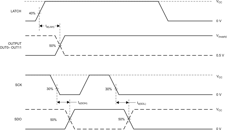 Figure 2. Output Signal Delay Time
6.8 Typical Characteristics
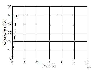
| VCC = 3.3 V | R(IREF) = 12.2 kΩ | TA = 25ºC |
| Dot correction = 255 | ||
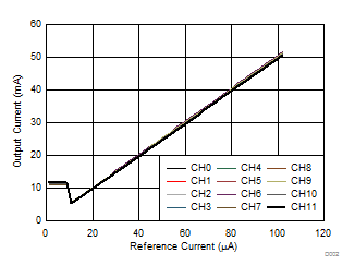
| VCC = 5.5 V | TA = 25ºC | Dot correction = 255 |
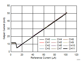
| VCC = 5.5 V | TA = 125ºC | Dot correction = 255 |
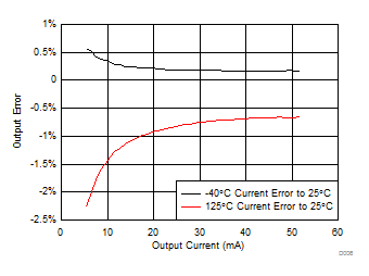
| VCC = 5.5 V | TA = 25ºC | Dot correction = 255 |
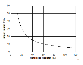
| VCC = 5.5 V | VO = 0.7 V | Dot correction = 255 |
| TA = 25ºC |
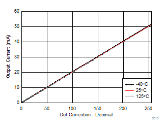
| VO = 0.7 V | IO = 51.4 mA | |
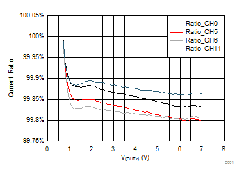
| VCC = 5.5 V | TA = 25ºC | R(IREF) = 12.2 kΩ |
| Dot correction = 255 | ||
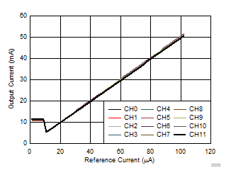
| VCC = 5.5 V | TA = –40ºC | Dot correction = 255 |
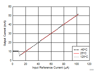
| VCC = 5.5 V | Channel = IOUT5 | Dot correction = 255 |
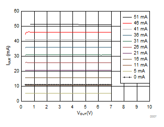
| VCC = 5.5 V | TA = 25ºC | Dot correction = 255 |
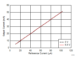
| VO = 0.7 V | TA = 25ºC | Dot correction = 255 |
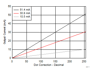
| VO = 0.7 V | TA = 25ºC | |