SLIS142D December 2012 – September 2016 TLC6C598-Q1
PRODUCTION DATA.
- 1 Features
- 2 Applications
- 3 Description
- 4 Revision History
- 5 Pin Configuration and Functions
- 6 Specifications
- 7 Parameter Measurement Information
- 8 Detailed Description
- 9 Application and Implementation
- 10Power Supply Recommendations
- 11Layout
- 12Device and Documentation Support
- 13Mechanical, Packaging, and Orderable Information
1 Features
- Qualified for Automotive Applications
- AEC-Q100 Qualified With the Following Results:
- Device Temperature Grade 1: –40°C to 125°C Ambient Operating Temperature Range
- Device HBM ESD Classification Level H2
- Device CDM ESD Classification Level C3B
- Wide Vcc From 3 V to 5.5 V
- Output Maximum Rating of.40 V
- Eight Power DMOS Transistor Outputs of 50-mA Continuous Current With VCC = 5 V
- Thermal Shutdown Protection
- Enhanced Cascading for Multiple Stages
- All Registers Cleared With Single Input
- Low Power Consumption
- Slow Switching Time (tr and tf), Which Helps Significantly With Reducing EMI
- 16-Pin TSSOP-PW Package
- 16-Pin SOIC-D Package
2 Applications
- Instrumentation Cluster
- Tell-Tale Lamps
- LED Illumination and Control
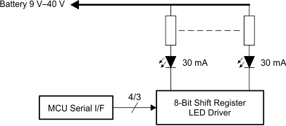
Typical Application Schematic

3 Description
The TLC6C598-Q1 is a monolithic, medium-voltage, low-current power 8-bit shift register designed for use in systems that require relatively moderate load power, such as LEDs.
This device contains an 8-bit serial-in, parallel-out shift register that feeds an 8-bit D-type storage register. Data transfers through both the shift and storage registers on the rising edge of the shift-register clock (SRCK) and the register clock (RCK), respectively. The storage register transfers data to the output buffer when shift register clear (CLR) is high. A low on CLR clears all registers in the device. Holding the output enable (G) high, holds all data in the output buffers low, and all drain outputs are off. Holding G low makes data from the storage register transparent to the output buffers. When data in the output buffers is low, the DMOS transistor outputs are off. When data is high, the DMOS transistor outputs have sink-current capability. The serial output (SER OUT) clocks out of the device on the falling edge of SRCK to provide additional hold time for cascaded applications. This provides improved performance for applications where clock signals may be skewed, devices are not located near one another, or the system must tolerate electromagnetic interference. The device contains built-in thermal shutdown protection.
Outputs are low-side, open-drain DMOS transistors with output ratings of 40 V and 50 mA continuous sink-current capabilities when Vcc = 5 V. The current limit decreases as the junction temperature increases for additional device protection. The device also provides up to 2000 V of ESD protection when tested using the human-body model and 200 V when using the machine model.
The TLC6C598-Q1 characterization is for for operation over the operating ambient temperature range of −40°C to 125°C.
Device Information(1)
| PART NUMBER | PACKAGE | BODY SIZE (NOM) |
|---|---|---|
| TLC6C598-Q1 | SOIC (16) | 9.90 mm x 3.91 mm |
| TSSOP (16) | 5.00 mm x 4.40 mm |
- For all available packages, see the orderable addendum at the end of the datasheet.