SLVS647I August   2006  – November 2014 TLE4275-Q1

UNLESS OTHERWISE NOTED, this document contains PRODUCTION DATA.  

  1. Features
  2. Applications
  3. Description
  4. Revision History
  5. Pin Configuration and Functions
  6. Specifications
    1. 6.1 Absolute Maximum Ratings
    2. 6.2 ESD Ratings
    3. 6.3 Recommended Operating Conditions
    4. 6.4 Thermal Information
    5. 6.5 Electrical Characteristics
    6. 6.6 Switching Characteristics
    7. 6.7 Typical Characteristics
  7. Parameter Measurement Information
  8. Detailed Description
    1. 8.1 Overview
    2. 8.2 Functional Block Diagram
    3. 8.3 Feature Description
      1. 8.3.1 Regulated Output (OUT)
      2. 8.3.2 Power-On-Reset (RESET)
      3. 8.3.3 Reset Delay Timer (DELAY)
    4. 8.4 Device Functional Modes
      1. 8.4.1 Low-Voltage Tracking
  9. Application and Implementation
    1. 9.1 Application Information
    2. 9.2 Typical Application
      1. 9.2.1 Design Requirements
      2. 9.2.2 Detailed Design Procedure
        1. 9.2.2.1 Power-Up Reset Capacitance
        2. 9.2.2.2 Thermal Consideration
      3. 9.2.3 Application Curves
  10. 10Power Supply Recommendations
  11. 11Layout
    1. 11.1 Layout Guidelines
    2. 11.2 Layout Example
  12. 12Device and Documentation Support
    1. 12.1 Documentation Support
      1. 12.1.1 Related Documentation
    2. 12.2 Trademarks
    3. 12.3 Electrostatic Discharge Caution
    4. 12.4 Glossary
  13. 13Mechanical, Packaging, and Orderable Information

Package Options

Refer to the PDF data sheet for device specific package drawings

Mechanical Data (Package|Pins)
  • KTT|5
  • PWP|20
  • KVU|5
Thermal pad, mechanical data (Package|Pins)
Orderable Information

5 Pin Configuration and Functions

KTT Package
5-Pin DDPAK/TO-263
Top View
TLE4275-Q1 po_5_ktt_slvs647.gif
KVU Package
5-Pin TO-252
Top View
TLE4275-Q1 po_5_kvu_slvs647.gif
PWP Package
20-Pin HTSSOP With Exposed Thermal Pad
Top View
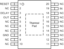
TLE4275-Q1 po_20_htssop_slvs647.gif

Pin Functions

PIN TYPE DESCRIPTION
NAME NO.
KTT KVU PWP
DELAY 4 4 3 O Reset delay. Connect to ground with a capacitor to set delay time.
GND 3 3 8 O Ground. Internally connected to heatsink
IN 1 1 19 I Input. Connect to ground as close to device as possible, through a ceramic capacitor.
NC 2, 5–7, 9–18, 20 Not connected
OUT 5 5 4 O Output. Connect to ground with ≥ 22-µF capacitor, ESR < 5 Ω at 10 kHz.
RESET 2 2 1 I Reset output. Open-collector output