SLVS647I August 2006 – November 2014 TLE4275-Q1
UNLESS OTHERWISE NOTED, this document contains PRODUCTION DATA.
- 1 Features
- 2 Applications
- 3 Description
- 4 Revision History
- 5 Pin Configuration and Functions
- 6 Specifications
- 7 Parameter Measurement Information
- 8 Detailed Description
- 9 Application and Implementation
- 10Power Supply Recommendations
- 11Layout
- 12Device and Documentation Support
- 13Mechanical, Packaging, and Orderable Information
Package Options
Refer to the PDF data sheet for device specific package drawings
Mechanical Data (Package|Pins)
- KTT|5
- PWP|20
- KVU|5
Thermal pad, mechanical data (Package|Pins)
Orderable Information
6 Specifications
6.1 Absolute Maximum Ratings(1)
over operating free-air temperature range (unless otherwise noted)| MIN | MAX | UNIT | |||
|---|---|---|---|---|---|
| VI | Input voltage range(2) | IN | –42 | 45 | V |
| DELAY | –0.3 | 7 | |||
| VO | Output voltage range | OUT | –1 | 16 | V |
| RESET | –0.3 | 25 | |||
| II | Input current | DELAY | ±2 | mA | |
| IO | Output current | RESET | ±5 | mA | |
| TJ | Operating junction temperature | –40 | 150 | °C | |
| Tstg | Storage temperature | –65 | 150 | °C | |
(1) Stresses beyond those listed under Absolute Maximum Ratings may cause permanent damage to the device. These are stress ratings only, and functional operation of the device at these or any other conditions beyond those indicated under Recommended Operating Conditions is not implied. Exposure to absolute-maximum-rated conditions for extended periods may affect device reliability.
(2) All voltage values are with respect to the network ground terminal.
(3) MM ESD rating tested per JESD22-A115.
6.2 ESD Ratings
| VALUE | UNIT | ||||
|---|---|---|---|---|---|
| V(ESD) | Electrostatic discharge | Human body model (HBM), per AEC Q100-002(1) | 6000 | V | |
| Machine model (MM)(3) | 400 | ||||
(1) AEC Q100-002 indicates HBM stressing is done in accordance with the ANSI/ESDA/JEDEC JS-001 specification.
6.3 Recommended Operating Conditions
over operating free-air temperature range (unless otherwise noted)| MIN | MAX | UNIT | ||
|---|---|---|---|---|
| VI | Input voltage | 5.5 | 42 | V |
| TJ | Junction temperature | –40 | 150 | °C |
6.4 Thermal Information
| THERMAL METRIC(1) | TLE4275-Q1 | UNIT | |||
|---|---|---|---|---|---|
| KTT | KVU | PWP | |||
| 5 PINS | 5 PINS | 20 PINS | |||
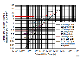
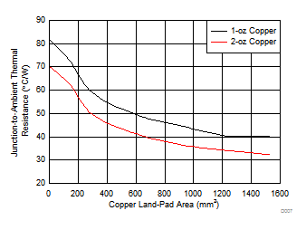
| RθJA | Junction-to-ambient thermal resistance | 32.8 | 40.3 | 39.3 | °C/W |
| RθJC(top) | Junction-to-case (top) thermal resistance | 38.0 | 31.8 | 22.7 | |
| RθJB | Junction-to-board thermal resistance | 5.3 | 17.2 | 19.1 | |
| ψJT | Junction-to-top characterization parameter | 6.3 | 2.8 | 0.6 | |
| ψJB | Junction-to-board characterization parameter | 5.4 | 17.1 | 18.9 | |
| RθJC(bot) | Junction-to-case (bottom) thermal resistance | 0.8 | 0.7 | 1.5 | |
(1) For more information about traditional and new thermal metrics, see the IC Package Thermal Metrics application report (SPRA953) .
6.5 Electrical Characteristics
over recommended operating free-air temperature range, VI = 13.5 V, TJ = −40°C to 150°C (unless otherwise noted) (see Figure 18)| PARAMETER | TEST CONDITIONS | MIN | TYP | MAX | UNIT | ||
|---|---|---|---|---|---|---|---|
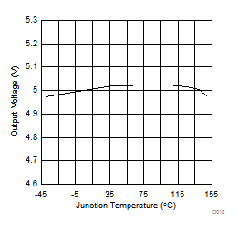
| VO | Output voltage | IO = 5 mA to 400 mA, VI = 6 V to 28 V | 4.9 | 5 | 5.1 | V | |
| IO = 5 mA to 200 mA, VI = 6 V to 40 V | 4.9 | 5 | 5.1 | ||||
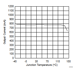
| IO | Output current limit | 450 | 700 | 950 | mA | ||
| Iq | Current consumption, Iq = II − IO | IO = 1 mA | TJ = 25°C | 150 | 200 | μA | |
| TJ ≤ 85°C | 150 | 220 | |||||
| IO = 250 mA | 5 | 10 | mA | ||||
| IO = 400 mA | 12 | 22 | |||||
| VDO | Dropout voltage(1) | IO = 300 mA, Vdo = VI − VO | 250 | 500 | mV | ||
| Load regulation | IO = 5 mA to 400 mA | 15 | 30 | mV | |||
| Line regulation | ΔVI = 8 V to 32 V, IO = 5 mA | –15 | 5 | 15 | mV | ||
| PSRR | Power-supply ripple rejection | fr = 100 Hz, Vr = 0.5 Vpp | 60 | dB | |||
 |
Temperature output-voltage drift | 0.5 | mV/K | ||||
| VO,rt | RESET switching threshold | 4.5 | 4.65 | 4.8 | V | ||
| VROL | RESET output low voltage | Rext ≥ 5 kΩ, VO > 1 V | 0.2 | 0.4 | V | ||
| IROH | RESET output leakage current | VROH = 5 V | 0 | 10 | μA | ||
| ID,c | RESET charging current | VD = 1 V | 3 | 5.5 | 9 | μA | |
| VDU | RESET upper timing threshold | 1.5 | 1.8 | 2.2 | V | ||
| VDRL | RESET lower timing threshold | 0.2 | 0.4 | 0.7 | V | ||
(1) Measured when the output voltage VO has dropped 100 mV from the nominal value obtained at VI = 13.5 V
6.6 Switching Characteristics
over operating free-air temperature range (unless otherwise noted) (see Figure 1)| PARAMETER | TEST CONDITIONS | MIN | TYP | MAX | UNIT | |
|---|---|---|---|---|---|---|
| trd | RESET delay time | CD = 47 nF | 10 | 16 | 22 | ms |
| trr | RESET reaction time | CD = 47 nF | 0.5 | 2 | µs | |
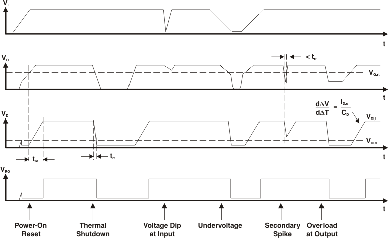 Figure 1. Reset Timing Diagram
6.7 Typical Characteristics
At TA = 25ºC
| VI = 6 V |
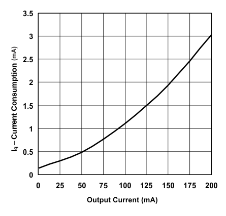
| VI = 13.5 V |
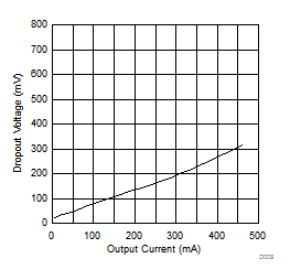
| TJ = 25°C |
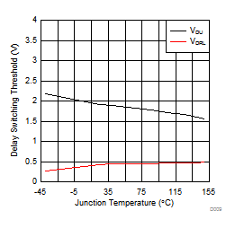
| VI = 13.5 V |
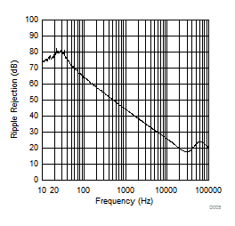
| VI = 13.5 V | Load = 200 mA | COUT = 22 µF |
| VI = 28 V |
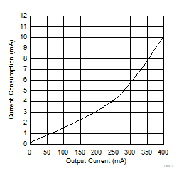
| VI = 13.5 V |
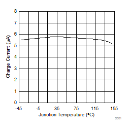
| VI = 13.5 V | VD = 1 V |
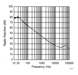
| VI = 13.5 V | Load = 1 mA | COUT = 22 µF |
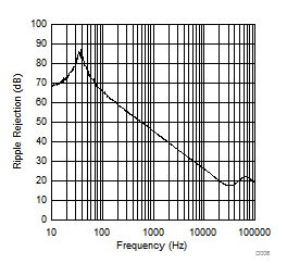
| VI = 13.5 V | Load = 400 mA | COUT = 22 µF |
