SBVS160C May 2011 – January 2023 TLV1117LV
PRODUCTION DATA
- 1 Features
- 2 Applications
- 3 Description
- 4 Revision History
- 5 Pin Configuration and Functions
- 6 Specifications
- 7 Detailed Description
- 8 Application and Implementation
- 9 Device and Documentation Support
- 10Mechanical, Packaging, and Orderable Information
Package Options
Mechanical Data (Package|Pins)
- DCY|4
Thermal pad, mechanical data (Package|Pins)
- DCY|4
Orderable Information
3 Description
The TLV1117LV low-dropout (LDO) linear regulator is a low input voltage version of the popular TLV1117 voltage regulator.
The TLV1117LV is an extremely low-power device that consumes 500 times lower quiescent current than traditional 1117 voltage regulators, making the device designed for applications that mandate very low standby current. The TLV1117LV LDO is also stable with 0 mA of load current; there is no minimum load requirement, making the device a good choice for applications where the regulator must power very small loads during standby in addition to large currents on the order of 1 A during normal operation. The TLV1117LV offers excellent line and load transient performance, resulting in very small magnitude undershoots and overshoots of output voltage when the load current requirement changes from less than 1 mA to more than 500 mA.
A precision band-gap and error amplifier provides 1.5% accuracy. A very high power-supply rejection ratio (PSRR) enables use of the device for post-regulation after a switching regulator. Other valuable features include low output noise and low-dropout voltage.
The device is internally compensated to be stable with 0-Ω equivalent series resistance (ESR) capacitors. These key advantages enable the use of cost-effective, small-size ceramic capacitors. Cost-effective capacitors that have higher bias voltages and temperature derating can also be used if desired.
The TLV1117LV is available in a SOT-223 package.
| PART NUMBER | PACKAGE(1) | BODY SIZE (NOM) |
|---|---|---|
| TLV1117LV | DCY (SOT-223, 4) | 6.50 mm × 3.50 mm |
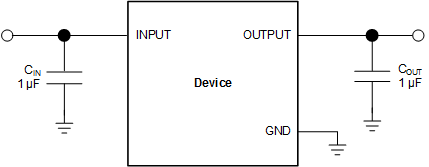
 Typical Application Circuit