SNOSD52B August   2018  – January 2020 TLV1805-Q1

PRODUCTION DATA.  

  1. Features
  2. Applications
  3. Description
    1.     Device Images
      1.      Reverse Current Protection Using an N-Channel MOSFET
      2.      Reverse Current & Overvoltage Protection Using P-Channel MOSFETs
  4. Revision History
  5. Pin Configuration and Functions
    1.     Pin Functions
  6. Specifications
    1. 6.1 Absolute Maximum Ratings
    2. 6.2 ESD Ratings
    3. 6.3 Recommended Operating Conditions
    4. 6.4 Thermal Information
    5. 6.5 Electrical Characteristics
    6. 6.6 Switching Characteristics
    7. 6.7 Typical Characteristics
  7. Detailed Description
    1. 7.1 Overview
    2. 7.2 Functional Block Diagram
    3. 7.3 Feature Description
      1. 7.3.1 Rail to Rail Inputs
      2. 7.3.2 Power On Reset
      3. 7.3.3 High Power Push-Pull Output
      4. 7.3.4 Shutdown Function
      5. 7.3.5 Internal Hysteresis
    4. 7.4 Device Functional Modes
      1. 7.4.1 External Hysteresis
        1. 7.4.1.1 Inverting Comparator With Hysteresis
        2. 7.4.1.2 Noninverting Comparator With Hysteresis
  8. Application and Implementation
    1. 8.1 Application Information
    2. 8.2 Typical Applications
      1. 8.2.1 Design Requirements
      2. 8.2.2 Detailed Design Procedure
      3. 8.2.3 Application Curve
      4. 8.2.4 Reverse Current Protection Using MOSFET and TLV1805-Q1
        1. 8.2.4.1 Minimum Reverse Current
        2. 8.2.4.2 N-Channel Reverse Current Protection Circuit
          1. 8.2.4.2.1 N-Channel Oscillator Circuit
      5. 8.2.5 P-Channel Reverse Current Protection Circuit
      6. 8.2.6 P-Channel Reverse Current Protection With Overvotlage Protection
      7. 8.2.7 ORing MOSFET Controller
  9. Power Supply Recommendations
  10. 10Layout
    1. 10.1 Layout Guidelines
    2. 10.2 Layout Example
  11. 11Device and Documentation Support
    1. 11.1 Documentation Support
      1. 11.1.1 Related Documentation
    2. 11.2 Receiving Notification of Documentation Updates
    3. 11.3 Support Resources
    4. 11.4 Trademarks
    5. 11.5 Electrostatic Discharge Caution
    6. 11.6 Glossary
  12. 12Mechanical, Packaging, and Orderable Information

Package Options

Mechanical Data (Package|Pins)
Thermal pad, mechanical data (Package|Pins)
Orderable Information

Noninverting Comparator With Hysteresis

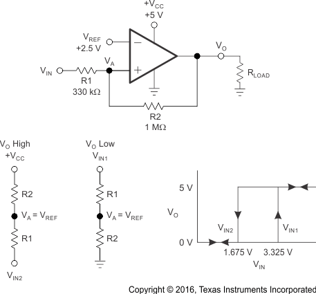
TLV1805-Q1 ai_noninverting_bos561.gifFigure 65. TLV1805-Q1 in a Noninverting Configuration With Hysteresis

A noninverting comparator with hysteresis requires a two-resistor network, as shown in Figure 65, and a voltage reference (VREF) at the inverting input. When VIN is low, the output is also low. For the output to switch from low to high, VIN must rise to VIN1. Use Equation 4 to calculate VIN1.

Equation 4. TLV1805-Q1 q_vin1_bos694.gif

When VIN is high, the output is also high. For the comparator to switch back to a low state, VIN must drop to VIN2 such that VA is equal to VREF. Use Equation 5 to calculate VIN2.

Equation 5. TLV1805-Q1 q_vin2_bos561.gif

The hysteresis of this circuit is the difference between VIN1 and VIN2, as shown in Equation 6.

Equation 6. TLV1805-Q1 q_delta_vin_bos561.gif