SNOSD50A December 2018 – January 2020 TLV1805
PRODUCTION DATA.
- 1 Features
- 2 Applications
- 3 Description
- 4 Revision History
- 5 Pin Configuration and Functions
- 6 Specifications
- 7 Detailed Description
-
8 Application and Implementation
- 8.1 Application Information
- 8.2 Typical Applications
- 9 Power Supply Recommendations
- 10Layout
- 11Device and Documentation Support
- 12Mechanical, Packaging, and Orderable Information
Package Options
Mechanical Data (Package|Pins)
- DBV|6
Thermal pad, mechanical data (Package|Pins)
Orderable Information
8.2.4 Reverse Current Protection Using MOSFET and TLV1805
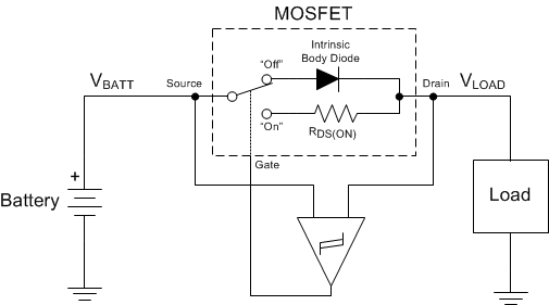
An N-Channel or P-Channel MOSFET may be used to protect against reverse current. Reverse current is defined as current flowing from the load (VLOAD) to the source (VBATT). Both the P-Channel and N-Channel circuits work on the same basic principle, where a comparator monitors the voltage across the MOSFET's Source and Drain terminals (monitoring VDS). The described circuits also protect against reverse voltage.
 Figure 68. Simplified Operational Theory
 When the current is flowing from the battery (VBATT) to the load (VLOAD), the battery voltage will be higher than the load voltage due to voltage drop across the MOSFET caused by the RDS(ON) or the intrinsic body diode forward voltage drop. The comparator will detect this and turn "on" the MOSFET so that the load current is now flowing through the low loss RDS(ON) path.
In a reverse current condition, VLOAD will be higher than VBATT. The comparator will detect this and drive the gate to set VGS = 0 to turn "off" the MOSFET (non-conducting). The body diode is reverse biased and will block current flow.
For a P-Channel MOSFET, the gate must be driven at least 4V or more below the battery voltage to turn "on" the MOSFET.
For a N-Channel MOSFET, the gate must be driven 4V or more above the battery voltage to turn "on" the MOSFET. If a higher voltage is not available in the system, a charge pump is usually required to generate a voltage higher than the battery voltage to provide the necessary positive gate drive voltage.