SNOSDC9B October 2022 – September 2023 TLV1811-Q1 , TLV1812-Q1 , TLV1814-Q1 , TLV1821-Q1 , TLV1822-Q1 , TLV1824-Q1
PRODMIX
- 1
- 1 Features
- 2 Applications
- 3 Description
- 4 Revision History
- 5 Pin Configuration and Functions
- 6 Specifications
- 7 Typical Characteristics
- 8 Detailed Description
-
9 Application and Implementation
- 9.1 Application Information
- 9.2 Typical Applications
- 9.3 Power Supply Recommendations
- 9.4 Layout
- 10Device and Documentation Support
- 11Mechanical, Packaging, and Orderable Information
Package Options
Mechanical Data (Package|Pins)
Thermal pad, mechanical data (Package|Pins)
Orderable Information
3 Description
The TLV181x-Q1 and TLV182x-Q1 are a family of Automotive grade 40 Volt single, dual and quad channel comparators with multiple output options. The family offers rail-to-rail inputs with push-pull or open-drain output options. The family has an excellent speed-to-power combination with a propagation delay of 420 ns with a full supply voltage range of 2.4 V to 40 V with a quiescent supply current of only 5 μA per channel.
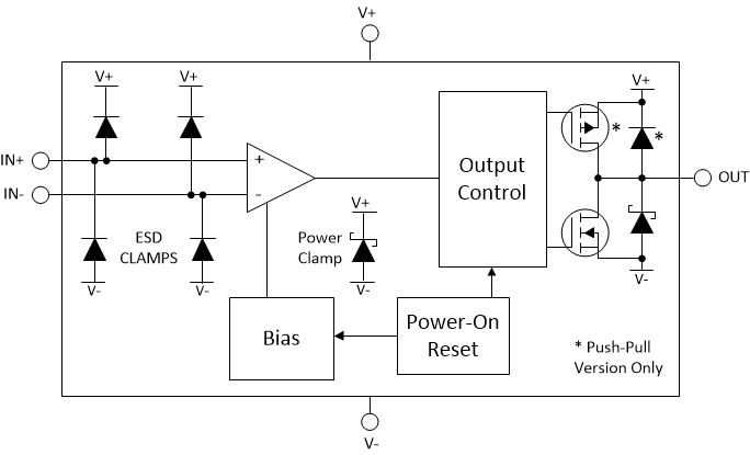
All devices include a Power-On Reset (POR) feature. This makes sure the output is in a known state until the minimum supply voltage has been reached before the output responds to the inputs, thus preventing false outputs during system power-up and power-down.
The TLV181x-Q1 comparators have a push-pull output stage capable of sinking and sourcing milliamps of current when controlling an LED or driving a capacitive load such as a MOSFET gate.
The TLV182x-Q1 comparators have an open-drain output stage that can be pulled up to 40 V independent of comparator supply voltage.
| PART NUMBER | PACKAGE (1) | BODY SIZE (NOM) |
|---|---|---|
| TLV1811-Q1, TLV1821-Q1 (Single) | SC-70 (5) | 1.25 mm x 2.00 mm |
| SOT-23 (5) | 1.60 mm x 2.90 mm | |
| TLV1811L-Q1, TLV1821L-Q1 | SOT-23 (5) | 1.60 mm x 2.90 mm |
| TLV1812-Q1, TLV1822-Q1 (Dual) | SOIC (8) | 3.91 mm × 4.90 mm |
| TSSOP (8) | 3.00 mm × 4.40 mm | |
| VSSOP (8) | 3.00 mm × 3.00 mm | |
| WSON (8) (Preview) | 2.00 mm × 2.00 mm | |
| SOT-23 (8) | 1.60 mm × 2.90 mm | |
| TLV1814-Q1, TLV1824-Q1 (Quad) | SOIC (14) | 3.91 mm × 8.65 mm |
| TSSOP (14) (Preview) | 4.40 mm × 5.00 mm | |
SOT-23 (14) (Preview) | 4.20 mm x 2.00 mm | |
| WQFN (16) (Preview) | 3.00 mm × 3.00 mm |
 TLV18xx-Q1 Block Diagram