SBOS884A October 2017 – December 2018 TLV2313-Q1 , TLV313-Q1
PRODUCTION DATA.
- 1 Features
- 2 Applications
- 3 Description
- 4 Revision History
- 5 Device Comparison Table
- 6 Pin Configuration and Functions
-
7 Specifications
- 7.1 Absolute Maximum Ratings
- 7.2 ESD Ratings
- 7.3 Recommended Operating Conditions
- 7.4 Thermal Information: TLV313-Q1
- 7.5 Thermal Information: TLV2313-Q1
- 7.6 Electrical Characteristics: 5.5 V
- 7.7 Electrical Characteristics: 1.8 V
- 7.8 Typical Characteristics: Table of Graphs
- 7.9 Typical Characteristics
- 8 Detailed Description
- 9 Application and Implementation
- 10Power Supply Recommendations
- 11Layout
- 12Device and Documentation Support
- 13Mechanical, Packaging, and Orderable Information
Package Options
Mechanical Data (Package|Pins)
Thermal pad, mechanical data (Package|Pins)
- DGK|8
Orderable Information
8.3.7 Input and ESD Protection
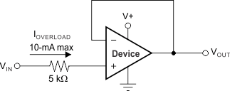
The TLVx313-Q1 family incorporates internal electrostatic discharge (ESD) protection circuits on all pins. In the case of input and output pins, this protection primarily consists of current-steering diodes connected between the input and power-supply pins. The ESD protection diodes also provide in-circuit, input overdrive protection, as long as the current is limited to 10 mA as stated in the Absolute Maximum Ratings. Figure 20 shows how a series input resistor may be added to the driven input to limit the input current. The added resistor contributes thermal noise at the amplifier input and the value must be kept to a minimum in noise-sensitive applications.
 Figure 20. Input Current Protection