SBOS837A November   2016  – January 2019 TLV2314-Q1 , TLV314-Q1 , TLV4314-Q1

PRODUCTION DATA.  

  1. Features
  2. Applications
  3. Description
    1.     Device Images
      1.      EMIRR vs Frequency
  4. Revision History
  5. Pin Configuration and Functions
    1.     Pin Functions: TLV314-Q1
    2.     Pin Functions: TLV2314-Q1
    3.     Pin Functions: TLV4314-Q1
  6. Specifications
    1. 6.1 Absolute Maximum Ratings
    2. 6.2 ESD Ratings
    3. 6.3 Recommended Operating Conditions
    4. 6.4 Thermal Information: TLV314-Q1
    5. 6.5 Thermal Information: TLV2314-Q1
    6. 6.6 Thermal Information: TLV4314-Q1
    7. 6.7 Electrical Characteristics
    8. 6.8 Typical Characteristics
    9. 6.9 Typical Characteristics
  7. Detailed Description
    1. 7.1 Overview
    2. 7.2 Functional Block Diagram
    3. 7.3 Feature Description
      1. 7.3.1 Operating Voltage
      2. 7.3.2 Rail-to-Rail Input
      3. 7.3.3 Rail-to-Rail Output
      4. 7.3.4 Common-Mode Rejection Ratio (CMRR)
      5. 7.3.5 Capacitive Load and Stability
      6. 7.3.6 EMI Susceptibility and Input Filtering
    4. 7.4 Device Functional Modes
  8. Application and Implementation
    1. 8.1 Application Information
    2. 8.2 Typical Application
      1. 8.2.1 Design Requirements
      2. 8.2.2 Detailed Design Procedure
      3. 8.2.3 Application Curve
    3. 8.3 System Examples
  9. Power Supply Recommendations
    1. 9.1 Input and ESD Protection
  10. 10Layout
    1. 10.1 Layout Guidelines
    2. 10.2 Layout Example
  11. 11Device and Documentation Support
    1. 11.1 Device Support
      1. 11.1.1 Development Support
    2. 11.2 Documentation Support
      1. 11.2.1 Related Documentation
    3. 11.3 Related Links
    4. 11.4 Community Resources
    5. 11.5 Trademarks
    6. 11.6 Electrostatic Discharge Caution
    7. 11.7 Glossary
  12. 12Mechanical, Packaging, and Orderable Information

Package Options

Mechanical Data (Package|Pins)
Thermal pad, mechanical data (Package|Pins)
Orderable Information

Input and ESD Protection

The TLVx314-Q1 family incorporates internal electrostatic discharge (ESD) protection circuits on all pins. In the case of input and output pins, this protection primarily consists of current-steering diodes connected between the input and power-supply pins. These ESD protection diodes provide in-circuit, input overdrive protection, as long as the current is limited to 10 mA, as stated in the Absolute Maximum Ratings table. Figure 19 shows how a series input resistor can be added to the driven input to limit the input current. The added resistor contributes thermal noise at the amplifier input, which must be kept to a minimum in noise-sensitive applications.
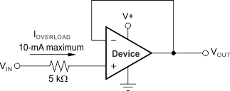
TLV314-Q1 TLV2314-Q1 TLV4314-Q1 inputcurrentprotectionSBOS837.gifFigure 19. Input Current Protection