SLAS510G March 2007 – February 2021 TLV320AIC3104
PRODUCTION DATA
- 1 Features
- 2 Applications
- 3 Description
- 4 Revision History
- 5 Description (Continued)
- 6 Device Comparison Table
- 7 Pin Configuration and Functions
- 8 Specifications
- 9 Parameter Measurement Information
-
10Detailed Description
- 10.1 Overview
- 10.2 Functional Block Diagrams
- 10.3
Feature Description
- 10.3.1 Hardware Reset
- 10.3.2 Digital Audio Data Serial Interface
- 10.3.3 Audio Data Converters
- 10.3.4 Stereo Audio DAC
- 10.3.5 Audio Analog Inputs
- 10.3.6 Analog Fully Differential Line Output Drivers
- 10.3.7 Analog High-Power Output Drivers
- 10.3.8 Input Impedance and VCM Control
- 10.3.9 MICBIAS Generation
- 10.3.10 Short-Circuit Output Protection
- 10.3.11 Jack and Headset Detection
- 10.4 Device Functional Modes
- 10.5 Programming
- 10.6 Register Maps
- 11Application and Implementation
- 12Power Supply Recommendations
- 13Layout
- 14Device and Documentation Support
Package Options
Refer to the PDF data sheet for device specific package drawings
Mechanical Data (Package|Pins)
- RHB|32
Thermal pad, mechanical data (Package|Pins)
- RHB|32
Orderable Information
10.3.11 Jack and Headset Detection
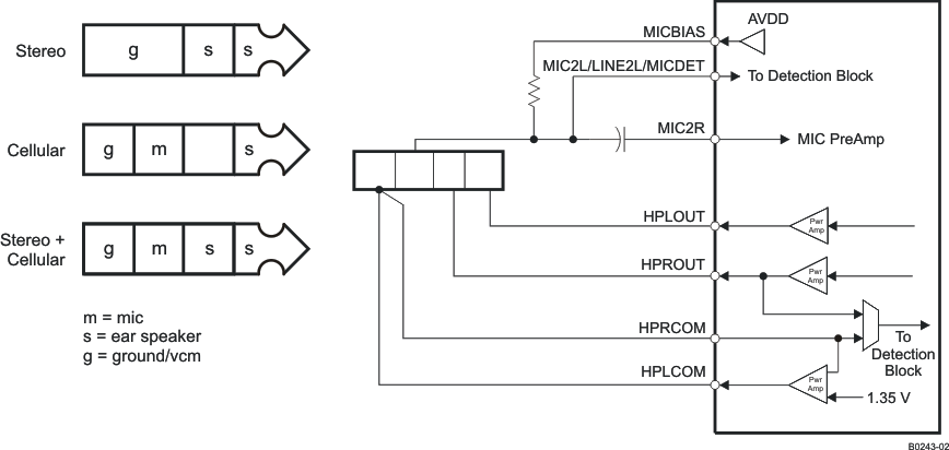
The TLV320AIC3104 includes extensive capability to monitor a headphone, microphone, or headset jack, determine if a plug has been inserted into the jack, and then determine what type of headset or headphone is wired to the plug. Figure 10-18 illustrates one configuration of the device that enables detection and determination of headset type when a pseudo-differential (capacitor free) stereo headphone output configuration is used. The registers used for this function are page 0, registers 14, 96, 97, and 13. The type of headset detected can be read back from page 0, register 13. Note that for best results, it is recommended to select a MICBIAS value as high as possible, and to program the output driver common-mode level at a 1.35-V or 1.5-V level.
 Figure 10-18 Configuration of Device for Jack Detection Using a Pseudo-Differential (Capacitor Free) Headphone Output Connection
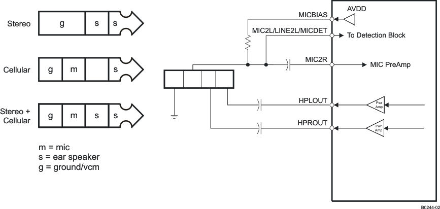
A modified output configuration used when the output drivers are ac-coupled is shown in Figure 10-19. In this mode, the device cannot accurately determine if the inserted headphone is a mono or stereo headphone.
 Figure 10-19 Configuration of Device for Jack Detection Using an AC-Coupled Stereo Headphone Output Connection
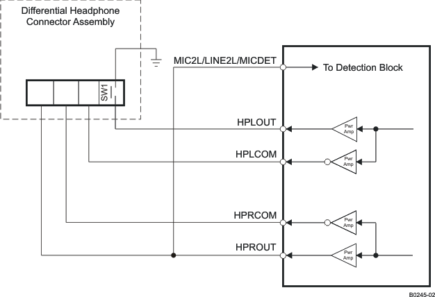
An output configuration for the case of the outputs driving fully differential stereo headphones is shown in Figure 10-20. In this mode, there is a requirement on the jack side that either HPLCOM or HPLOUT get shorted to ground if the plug is removed, which can be implemented using a spring terminal in a jack. For this mode to function properly, short-circuit detection should be enabled and configured to power down the drivers if a short-circuit is detected. The registers that control this functionality are in page 0, register 38, bits D2–D1.
 Figure 10-20 Configuration of Device for Jack Detection Using a Fully Differential Stereo Headphone Output Connection