SBOSAB8A June 2023 – December 2023 TLV365-Q1
PRODMIX
- 1
- 1 Features
- 2 Applications
- 3 Description
- 4 Device Comparison Table
- 5 Pin Configuration and Functions
- 6 Specifications
- 7 Detailed Description
- 8 Application and Implementation
- 9 Device and Documentation Support
- 10Revision History
- 11Mechanical, Packaging, and Orderable Information
Package Options
Refer to the PDF data sheet for device specific package drawings
Mechanical Data (Package|Pins)
- DBV|5
Thermal pad, mechanical data (Package|Pins)
Orderable Information
3 Description
The TLV365-Q1 and TLV2365-Q1 (TLVx365-Q1) devices are a family of zerø-crossover, rail-to-rail input and output, CMOS operational amplifiers, optimized for low voltage and cost-sensitive applications. Low-noise (4.5 nV/√Hz) and high-speed operation (50‑MHz gain bandwidth) make these devices an excellent choice for driving sampling analog-to-digital converters (ADCs) in applications such as low-side current sensing, audio, signal conditioning, and sensor amplification.
Special features include an excellent common-mode rejection ratio (CMRR), no input stage crossover distortion, high input impedance, and rail-to-rail input and output swing. The input common-mode range includes both the negative and positive supplies. The output voltage swings to within 12 mV of the rails.
The TLVx365-Q1 are specified for operation from −40°C to +125°C.
| PART NUMBER | CHANNEL COUNT | PACKAGE(1) |
|---|---|---|
| TLV365-Q1 | Single | DBV (SOT-23, 5) |
| TLV2365-Q1(2) | Dual | D (SOIC, 8) |
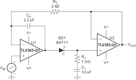
 Fast-Settling Peak
Detector
 TLVx365-Q1 for Current
Sensing