SNVSB04C March   2019  – December 2021 TLV4021 , TLV4031 , TLV4041 , TLV4051

PRODUCTION DATA  

  1. Features
  2. Applications
  3. Description
  4. Revision History
  5. Pin Configuration and Functions
  6. Specifications
    1. 6.1 Absolute Maximum Ratings
    2. 6.2 ESD Ratings
    3. 6.3 Recommended Operating Conditions
    4. 6.4 Thermal Information
    5. 6.5 Electrical Characteristics
    6. 6.6 Switching Characteristics
  7. Typical Characteristics
  8. Detailed Description
    1. 8.1 Overview
    2. 8.2 Functional Block Diagram
    3. 8.3 Feature Description
    4. 8.4 Device Functional Modes
      1. 8.4.1 Power ON Reset (POR)
      2. 8.4.2 Input (IN)
      3. 8.4.3 Switching Thresholds and Hysteresis (VHYS)
      4. 8.4.4 Output (OUT)
  9. Application and Implementation
    1. 9.1 Application Information
      1. 9.1.1 Monitoring (V+)
      2. 9.1.2 Monitoring a Voltage Other than (V+)
      3. 9.1.3 VPULLUP to a Voltage Other than (V+)
    2. 9.2 Typical Application
      1. 9.2.1 Under-Voltage Detection
        1. 9.2.1.1 Design Requirements
        2. 9.2.1.2 Detailed Design Procedure
        3. 9.2.1.3 Application Curve
      2. 9.2.2 Additional Application Information
        1. 9.2.2.1 Pull-up Resistor Selection
        2. 9.2.2.2 Input Supply Capacitor
        3. 9.2.2.3 Sense Capacitor
    3. 9.3 What to Do and What Not to Do
  10. 10Power Supply Recommendations
  11. 11Layout
    1. 11.1 Layout Guidelines
    2. 11.2 Layout Example
  12. 12Device and Documentation Support
    1. 12.1 Receiving Notification of Documentation Updates
    2. 12.2 Support Resources
    3. 12.3 Trademarks
    4. 12.4 Electrostatic Discharge Caution
    5. 12.5 Glossary
  13. 13Mechanical, Packaging, and Orderable Information

Package Options

Mechanical Data (Package|Pins)
Thermal pad, mechanical data (Package|Pins)
Orderable Information

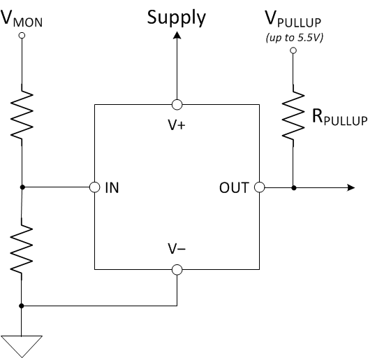
VPULLUP to a Voltage Other than (V+)

For applications where the output of the comparator needs to interface with a reset/enable pin that operates from a different supply voltage, the open-drain comparators (TLV4021/4031) should be selected. In these usage cases, the output can be pulled up to any voltage that is lower than 5.5V (independent of (V+)). This technique is commonly referred to as "level-shifting."
GUID-759B0254-FBC4-4F9E-BEBD-9EB66247A361-low.gifFigure 9-3 Level-Shifting