SNVSBU0 October 2020 TLV4062-Q1 , TLV4082-Q1
PRODUCTION DATA
- 1 Features
- 2 Applications
- 3 Description
- 4 Revision History
- 5 Pin Configuration and Functions
- 6 Specifications
- 7 Detailed Description
- 8 Application and Implementation
- 9 Power Supply Recommendations
- 10Layout
- 11Device and Documentation Support
Package Options
Mechanical Data (Package|Pins)
- DBV|6
Thermal pad, mechanical data (Package|Pins)
Orderable Information
8.2.1.2 Detailed Design Procedure
Configure the circuit as shown in Figure 8-1. Connect V+ to a power supply that is compatible with the input logic level of the device connected to the output, and connect V- to ground. Resistors R1 and R2 create the over-voltage alert level at 6.5 V and resistors R3 and R4 create the over-voltage alert level at 4 V. When the VMON rises, the resistor divider voltage crosses VIT+. This causes the comparator output to transition from a logic low level (normal operation), to a logic high level. When VMON falls back down and the resistor divider voltage crosses VIT- and signal that the system is approaching normal operating voltage levels once again. Make sure to set VMON at a value below the absolute maximum voltage of the system in question.
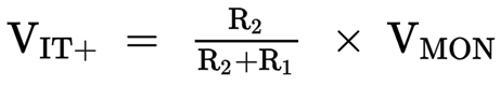
where
- R1/R3 and R2/R4 are the resistor values for the resistor divider connected to INx
- VMON is the voltage source that is being monitored for an over-voltage condition
- VIT+ is the rising edge threshold where the comparator output changes state from low to high
Rearranging Equation 2 and solving for R1 yields Equation 3. Set R2/R4 to a fixed value.
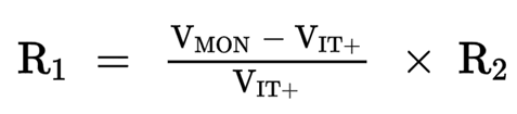
Using the nearest 1% resistors and the equation above, R1 = 300 kΩ, R2 =1.33 MΩ, R3 = 953 kΩ, and R4 = 407 kΩ. To get the trip point as close as possible to rising threshold, VIT+, VMON are adjusted so that VMON1 = 6.49 V and VMON2 = 3.99 V. Using equation Equation 4 will determine when the output will fall low (crossing VIT-). The over-voltage signal will go low when VMON1 = 6.16 V and VMON2 = 3.79 V.

where
- VMON is the voltage at which the resistor divider crosses the falling threshold, VIT-
Choose RTOTAL (equal to R1 + R2 & R3 + R4) so that the current through the divider is approximately 100 times higher than the input current at the INx pins. The resistors can have high values to minimize current consumption as a result of low input bias current without adding significant error to the resistive divider. For details on sizing input resistors, see the Optimizing Resistor Dividers at a Comparator Input application report (SLVA450), available for download from www.ti.com.