SNVSBU0 October 2020 TLV4062-Q1 , TLV4082-Q1
PRODUCTION DATA
- 1 Features
- 2 Applications
- 3 Description
- 4 Revision History
- 5 Pin Configuration and Functions
- 6 Specifications
- 7 Detailed Description
- 8 Application and Implementation
- 9 Power Supply Recommendations
- 10Layout
- 11Device and Documentation Support
Package Options
Mechanical Data (Package|Pins)
- DBV|6
Thermal pad, mechanical data (Package|Pins)
Orderable Information
8.2.2.2 Detailed Design Procedure
Configure the circuit as shown in Figure 8-3. Connect V+ to a 3.3 V power rail and connect V- to ground. The resistor network is used to create an early warning detection signal at OUT2, which will give a warning alert as VMON approaches the max limit, changing state from a logic low to a logic high. OUT2 will stay high for a longer period until VMON is no longer in the warning zone. OUT1 will be used when VMON reaches the max limit and transition from a logic low to a logic high. This type of topology can be used for sensitive systems where advanced notice of the power supply over-voltage detection is needed.
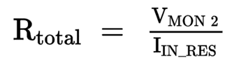
Use VMON2, the threshold for a low to high transition at OUT2, IIN_RES, the current flow through the resistor network, to determine the minimum total resistance necessary to achieve the current consumption specification.
where
- VMON2 is the target voltage at which OUT2 goes high when VMON rises
- IIN_RES is the current flowing through the resistor network
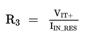
After RTOTAL is determined, R3 can be calculated using Equation 6. Select the nearest 1% resistor value for R3. In this case, 845 kΩ is the closest value.
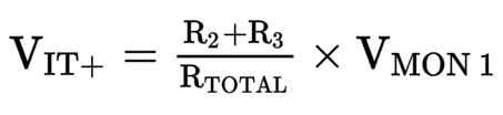
Use the voltage divider equation Equation 7 The voltage divider equation controls the V MON1 voltage at which OUT1 will transition from a logic high to a logic low.
where
- VMON1 is the target voltage at which OUT1 goes low when VMON falls
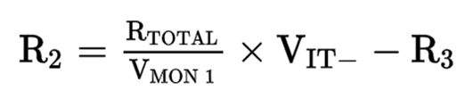
Rearranging Equation 7 to solve for R2 yields Equation 8 Select the nearest 1% resistor value for R2. In this case, 55.6kΩ is the closest value.
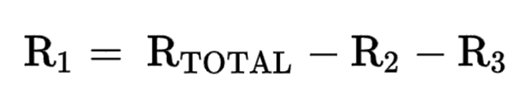
Use Equation 9 to calculate R1. Select the nearest 1% resistor value for R1. In this case, 1.87 MΩ is a 1% resistor.