SNVSBU0 October 2020 TLV4062-Q1 , TLV4082-Q1
PRODUCTION DATA
- 1 Features
- 2 Applications
- 3 Description
- 4 Revision History
- 5 Pin Configuration and Functions
- 6 Specifications
- 7 Detailed Description
- 8 Application and Implementation
- 9 Power Supply Recommendations
- 10Layout
- 11Device and Documentation Support
Package Options
Mechanical Data (Package|Pins)
- DBV|6
Thermal pad, mechanical data (Package|Pins)
Orderable Information
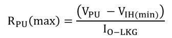
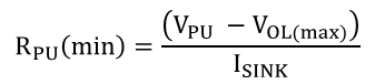
8.2.3.1 Pull-Up Resistor Selection
For the TLV4082-Q1 (open-drain outputs), care should be taken in selecting the pull-up resistor (RPU) value to ensure proper output voltage levels. First, consider the required output high logic level requirement of the logic device that is being drive by the comparator when calculating the maximum RPU value. When in a logic high output state, the output impedance of the comparator is very high but there is finite amount of leakage current that needs to be accounted for. Use the | Ilkg(OD)| from the EC table and the VIH (min) of the logic device being driven by the TLV4082 to determine RPU using Equation 10 .
Next determine the minimum value for RPU by using the VIL (max) of the logic device being driven by the TLV4082-Q1. In order for the comparator output to be recognized as a logic low, VIL (max) is used to determine the upper boundary of the comparator's VOL. VOL (max) for the comparator is available in the EC table from specific sink current levels and can be found from the VOUT versus ISINK curve in the Typical Applications curve. A good design practice is to choose a value for VOL that is ½ the value of VIL for the input logic device. The corresponding sink current and VOL value will be needed to calculate the minimum RPU. This method will ensure enough noise margin for the logic low level. With iSINK determined and the corresponding RPU obtained, the minimum ) is calculated with Equation 11.
Since the range of possible RPU values is large, a value between 5 kΩ and 100kΩ is generally recommended. A smaller RPU value provides faster output transition time and better noise immunity, while a larger RPU value consumes less power when in a logic low output state.