SBVS292C July   2016  – June 2018

PRODUCTION DATA.  

  1. Features
  2. Applications
  3. Description
    1.     Device Images
      1.      Typical Application Circuit (Fixed-Voltage Versions)
  4. Revision History
  5. Pin Configuration and Functions
    1.     Pin Functions
  6. Specifications
    1. 6.1 Absolute Maximum Ratings
    2. 6.2 ESD Ratings
    3. 6.3 Recommended Operating Conditions
    4. 6.4 Thermal Information
    5. 6.5 Electrical Characteristics
    6. 6.6 Typical Characteristics
  7. Detailed Description
    1. 7.1 Overview
    2. 7.2 Functional Block Diagram
    3. 7.3 Feature Description
      1. 7.3.1 Internal Current Limit
      2. 7.3.2 Shutdown
      3. 7.3.3 Dropout Voltage
      4. 7.3.4 Undervoltage Lockout (UVLO)
    4. 7.4 Device Functional Modes
      1. 7.4.1 Operation with VIN Less Than 2 V
      2. 7.4.2 Operation with VIN Greater Than 2 V
  8. Application and Implementation
    1. 8.1 Application Information
      1. 8.1.1 Input and Output Capacitor Requirements
      2. 8.1.2 Transient Response
      3. 8.1.3 Thermal Protection
    2. 8.2 Typical Application
      1. 8.2.1 Design Requirements
      2. 8.2.2 Detailed Design Procedure
        1. 8.2.2.1 Input Capacitance
        2. 8.2.2.2 Output Capacitance
        3. 8.2.2.3 Thermal Calculation
      3. 8.2.3 Application Curve
  9. Power Supply Recommendations
  10. 10Layout
    1. 10.1 Layout Guidelines
    2. 10.2 Board Layout Recommendations to Improve PSRR and Noise Performance
    3. 10.3 Layout Example
  11. 11Device and Documentation Support
    1. 11.1 Documentation Support
      1. 11.1.1 Related Documentation
    2. 11.2 Receiving Notification of Documentation Updates
    3. 11.3 Community Resources
    4. 11.4 Trademarks
    5. 11.5 Electrostatic Discharge Caution
    6. 11.6 Glossary
  12. 12Mechanical, Packaging, and Orderable Information

Package Options

Mechanical Data (Package|Pins)
Thermal pad, mechanical data (Package|Pins)
Orderable Information

Typical Characteristics

at TJ = –40°C to +125°C, VIN = VOUT(TYP) + 0.5 V or 2 V (whichever is greater), IOUT = 10 mA, VEN = VIN, CIN = 1 µF, and COUT = 1 µF (unless otherwise noted); typical values are at TJ = 25°C
TLV700xx-Q1 Line_Reg_10mA.gif
Figure 1. TLV70028-Q1 Line Regulation
TLV700xx-Q1 Load_Reg.gif
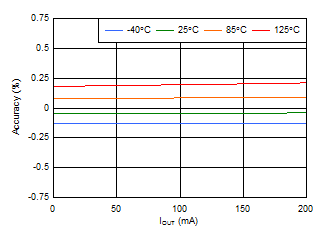
Figure 3. TLV70028-Q1 Load Regulation
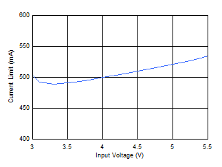
TLV700xx-Q1 Icl_Vin.gif
Figure 5. TLV70028-Q1 Current Limit vs Input Voltage
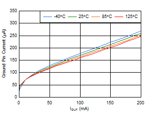
TLV700xx-Q1 Ignd_Load.gif
Figure 7. TLV70028-Q1 Ground Pin Current vs Output Current
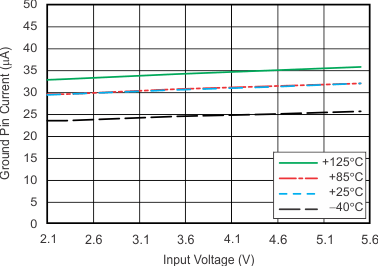
TLV700xx-Q1 tc_ignd_vin_0ma_sbvs292.gif
IOUT = 0 mA
Figure 9. TLV70048-Q1 Ground Pin Current vs Input Voltage
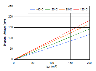
TLV700xx-Q1 Vdo_Load.gif
Figure 11. TLV70028-Q1 Dropout Voltage vs Output Current
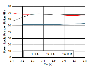
TLV700xx-Q1 tc_PSRR_vs_Vin.gif
Figure 13. TLV70028-Q1 Power-Supply Rejection Ratio vs Output Voltage
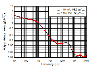
TLV700xx-Q1 tc_Noise_vs_Iout_TLV700.gif
Figure 15. TLV70028-Q1 Output Spectral Noise Density vs Frequency
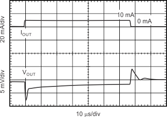
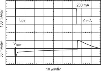
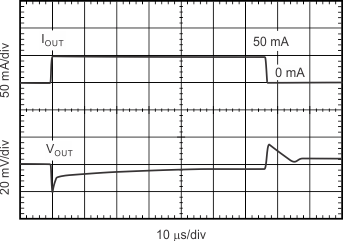
TLV700xx-Q1 tc_load_tr_10_sbvs292.gif
tR = tF = 1 µs, VIN = 2.3 V
Figure 17. Load Transient Response
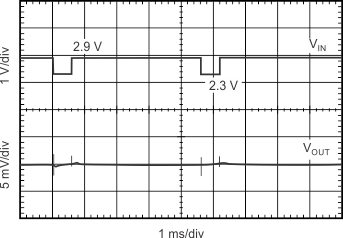
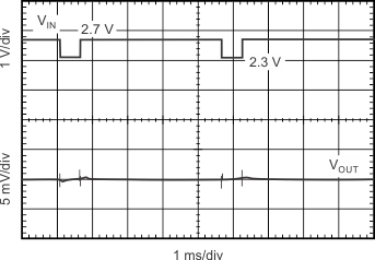
TLV700xx-Q1 tc_line_tr_200-1_sbvs292.gif
Slew rate = 1 V/µs, IOUT = 200 mA
Figure 19. Line Transient Response
TLV700xx-Q1 tc_line_tr_200-2_sbvs292.gif
Slew rate = 1 V/µs, IOUT = 200 mA
Figure 21. Line Transient Response
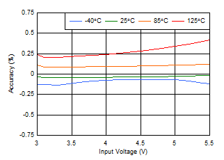
TLV700xx-Q1 Line_Reg_200mA.gif
Figure 2. TLV70028-Q1 Line Regulation
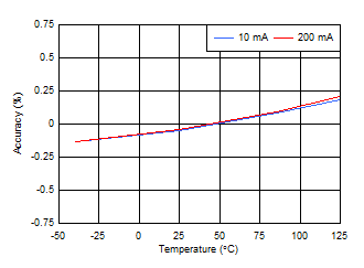
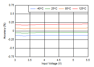
TLV700xx-Q1 Accuracy_Temp.gif
Figure 4. TLV70028-Q1 Accuracy vs Temperature
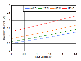
TLV700xx-Q1 Shutdown_Vin.gif
Figure 6. TLV70028-Q1 Shutdown Current vs Input Voltage
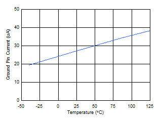
TLV700xx-Q1 Ignd_Temp.gif
Figure 8. TLV70028-Q1 Ground Pin Current vs Temperature
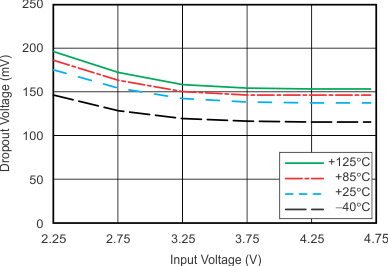
TLV700xx-Q1 tc_vdo_vin_sbvs292.gif
IOUT = 200 mA
Figure 10. TLV70048-Q1 Dropout Voltage vs Input Voltage
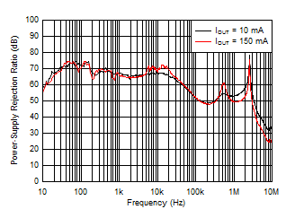
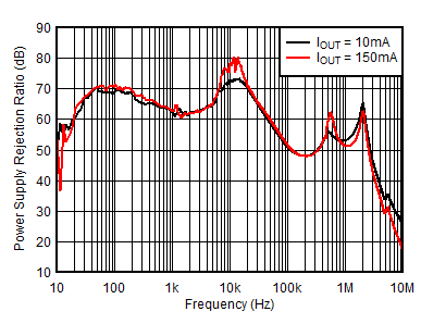
TLV700xx-Q1 tc_PSRR_vs_Freq.gif
Figure 12. TLV70028-Q1 Power-Supply Rejection Ratio vs Frequency
TLV700xx-Q1 TLV700-Q1_3.3VPSRR.gif
Figure 14. TLV70033-Q1 PSRR Ratio
TLV700xx-Q1 tc_load_tr_150_sbvs292.gif
tR = tF = 1 µs, VIN = 2.1 V
Figure 16. Load Transient Response
TLV700xx-Q1 tc_load_tr_50_sbvs292.gif
tR = tF = 1 µs, VIN = 2.3 V
Figure 18. Load Transient Response
TLV700xx-Q1 tc_line_tr_1_sbvs292.gif
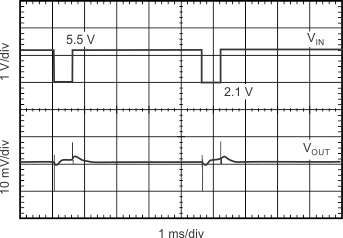
Slew rate = 1 V/µs, IOUT = 200 mA
Figure 20. Line Transient Response