SNOSDA5D May 2020 – February 2023 TLV7031-Q1 , TLV7032-Q1 , TLV7034-Q1 , TLV7041-Q1 , TLV7042-Q1 , TLV7044-Q1
PRODUCTION DATA
- 1 Features
- 2 Applications
- 3 Description
- 4 Revision History
- 5 Pin Configuration and Functions
-
6 Specifications
- 6.1 Absolute Maximum Ratings
- 6.2 ESD Ratings
- 6.3 Recommended Operating Conditions
- 6.4 Thermal Information (Single)
- 6.5 Thermal Information (Dual)
- 6.6 Thermal Information (Quad)
- 6.7 Electrical Characteristics
- 6.8 Switching Characteristics
- 6.9 Electrical Characteristics (Dual)
- 6.10 Switching Characteristics (Dual)
- 6.11 Electrical Characteristics (Quad)
- 6.12 Switching Characteristics (Quad)
- 6.13 Timing Diagrams
- 6.14 Typical Characteristics
- 7 Detailed Description
- 8 Application and Implementation
- 9 Power Supply Recommendations
- 10Layout
- 11Device and Documentation Support
- 12Mechanical, Packaging, and Orderable Information
Package Options
Mechanical Data (Package|Pins)
- PW|14
Thermal pad, mechanical data (Package|Pins)
- PW|14
Orderable Information
8.1.1 Inverting Comparator With Hysteresis for TLV703x-Q1
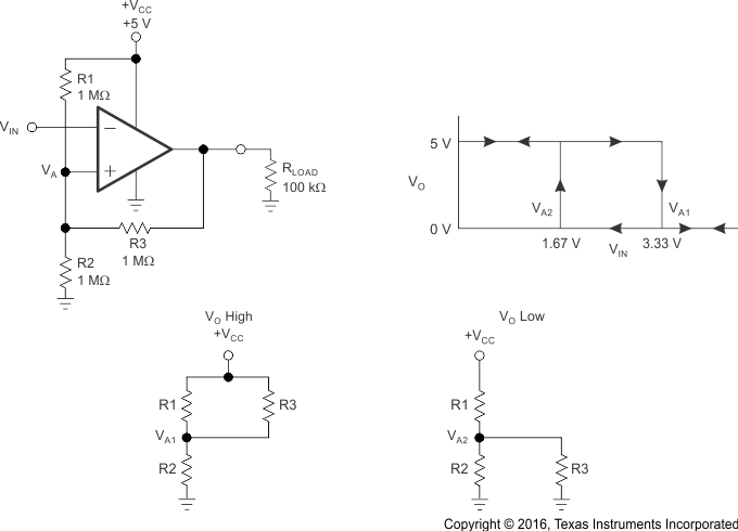
The inverting comparator with hysteresis requires a three-resistor network that is referenced to the comparator supply voltage (VCC), as shown in Figure 8-1. When VIN at the inverting input is less than VA, the output voltage is high (for simplicity, assume VO switches as high as VCC). The three network resistors can be represented as R1 || R3 in series with R2. Equation 1 defines the high-to-low trip voltage (VA1).

When VIN is greater than VA, the output voltage is low, very close to ground. In this case, the three network resistors can be presented as R2 || R3 in series with R1. Use Equation 2 to define the low to high trip voltage (VA2).

Equation 3 defines the total hysteresis provided by the network.

 Figure 8-1 TLV703x-Q1 in an
Inverting Configuration With Hysteresis