SBVS195F September   2012  – August 2019 TLV713

PRODUCTION DATA.  

  1. Features
  2. Applications
  3. Description
    1.     Device Images
      1.      Typical Application Circuit
      2.      Dropout Voltage vs Output Current
  4. Revision History
  5. Pin Configurations and Functions
    1.     Pin Functions
  6. Specifications
    1. 6.1 Absolute Maximum Ratings
    2. 6.2 ESD Ratings
    3. 6.3 Recommended Operating Conditions
    4. 6.4 Thermal Information
    5. 6.5 Electrical Characteristics
    6. 6.6 Typical Characteristics
  7. Detailed Description
    1. 7.1 Overview
    2. 7.2 Functional Block Diagrams
    3. 7.3 Feature Description
      1. 7.3.1 Undervoltage Lockout (UVLO)
      2. 7.3.2 Shutdown
      3. 7.3.3 Foldback Current Limit
      4. 7.3.4 Thermal Protection
    4. 7.4 Device Functional Modes
      1. 7.4.1 Normal Operation
      2. 7.4.2 Dropout Operation
      3. 7.4.3 Disabled
  8. Application and Implementation
    1. 8.1 Application Information
      1. 8.1.1 Input and Output Capacitor Considerations
      2. 8.1.2 Dropout Voltage
      3. 8.1.3 Transient Response
      4. 8.1.4 UVLO Circuit Limitation
    2. 8.2 Typical Application
      1. 8.2.1 Design Requirements
      2. 8.2.2 Detailed Design Procedure
      3. 8.2.3 Application Curves
    3. 8.3 What to Do and What Not to Do
  9. Power Supply Recommendations
  10. 10Layout
    1. 10.1 Layout Guidelines
      1. 10.1.1 Board Layout Recommendations to Improve PSRR and Noise Performance
      2. 10.1.2 Power Dissipation
    2. 10.2 Layout Examples
  11. 11Device and Documentation Support
    1. 11.1 Device Support
      1. 11.1.1 Development Support
        1. 11.1.1.1 Evaluation Modules
        2. 11.1.1.2 Spice Models
      2. 11.1.2 Device Nomenclature
    2. 11.2 Documentation Support
      1. 11.2.1 Related Documentation
    3. 11.3 Receiving Notification of Documentation Updates
    4. 11.4 Community Resources
    5. 11.5 Trademarks
    6. 11.6 Electrostatic Discharge Caution
    7. 11.7 Glossary
  12. 12Mechanical, Packaging, and Orderable Information

Package Options

Mechanical Data (Package|Pins)
Thermal pad, mechanical data (Package|Pins)
Orderable Information

Pin Configurations and Functions

DQN Package
4-Pin X2SON
Top View
TLV713 po_dfn_dpw_bvs195.gif
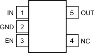
DBV Package
5-Pin SOT-23
Top View
TLV713 po_sot23_bvs195.gif

Pin Functions

PIN I/O DESCRIPTION
NAME NO.
X2SON SOT-23
EN 3 3 I Enable pin. Driving EN over 0.9 V turns on the regulator.
Driving EN below 0.4 V puts the regulator into shutdown mode.
GND 2 2 Ground pin
IN 4 1 I Input pin. A small capacitor is recommended from this pin to ground. See the Input and Output Capacitor Considerations section in the Feature Description for more details.
NC 4 No internal connection
OUT 1 5 O Regulated output voltage pin. For best transient response, a small 1-μF ceramic capacitor is recommended from this pin to ground. See the Input and Output Capacitor Considerations section in the Feature Description for more details.
Thermal pad The thermal pad is electrically connected to the GND node. Connect to the GND plane for improved thermal performance.