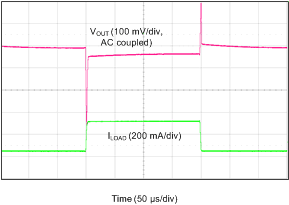
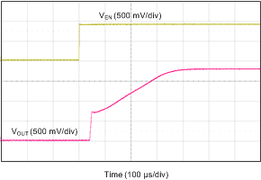
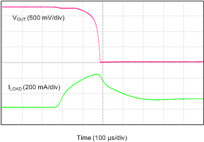
at operating temperature range (TJ = –40°C to +150°C), VIN = VOUT(nom) + 0.5 V or 2.0 V (whichever is greater), IOUT = 1 mA, VEN = VIN, and CIN = COUT = 1 µF (unless otherwise noted)
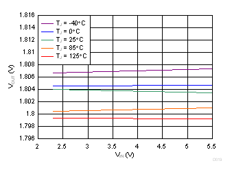 Figure 6-1 1.8-V
Regulation vs VIN (Line Regulation) and Temperature
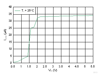 Figure 6-3 Ground Pin Current vs VIN
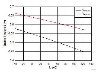 Figure 6-5 Enable Threshold vs Temperature
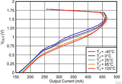 Figure 6-7 Output Voltage vs 1.8-V Foldback Current Limit and Temperature
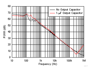 Figure 6-9 Power-Supply Rejection Ratio vs Frequency
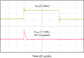
| IOUT = 10 mA, 1-µF output capacitor |
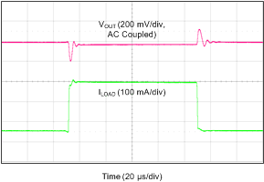
| VIN = 2.0 V, 1-µF output capacitor, output current slew rate = 0.25 A/µs |
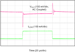
| VIN = 3.8 V,1-µF output capacitor, output current slew rate = 0.25 A/µs |
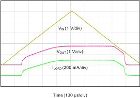
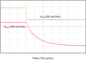
| RL = 6.2 Ω, VEN = VIN, 1-µF output capacitor |
| IOUT = 300 mA, 1-µF output capacitor |
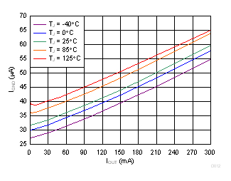 Figure 6-2 Ground Pin Current vs IOUT and Temperature
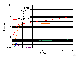 Figure 6-4 Shutdown Current vs VIN and Temperature
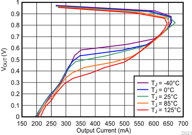 Figure 6-6 Output Voltage vs 1.0-V Foldback Current Limit and Temperature
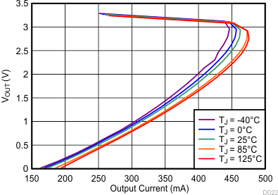
 Figure 6-8 Output Voltage vs 3.3-V Foldback Current Limit and Temperature
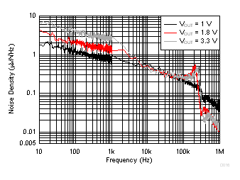
 Figure 6-10 Output Spectral Noise Density vs Frequency and Output Voltage
| IOUT = 300 mA, 1-µF output capacitor |

VIN = 2.0 V, no output capacitor,
output current slew rate =
0.25 A/µs |

VIN = 3.8 V, no output capacitor, output
current slew rate =
0.25
A/µs |
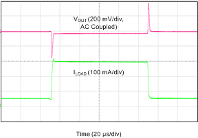
Figure 6-16 3.3
V, 50-mA to 300-mA Load Transient
| RL = 6.2 Ω, 1-µF output capacitor |
 Figure 6-20 Foldback Current Limit Response
 Figure 6-1 1.8-V
Regulation vs VIN (Line Regulation) and Temperature
 Figure 6-5 Enable Threshold vs Temperature


 Figure 6-2 Ground Pin Current vs IOUT and Temperature
 Figure 6-6 Output Voltage vs 1.0-V Foldback Current Limit and Temperature