SBVS157E April 2011 – December 2020 TLV803 , TLV853
PRODUCTION DATA
- 1 Features
- 2 Applications
- 3 Description
- 4 Revision History
- 5 Device Comparison
- 6 Pin Configuration and Functions
- 7 Specifications
- 8 Detailed Description
- 9 Application and Implementation
- 10Power Supply Recommendations
- 11Layout
- 12Device and Documentation Support
- 13Mechanical, Packaging, and Orderable Information
Package Options
Mechanical Data (Package|Pins)
- DBZ|3
Thermal pad, mechanical data (Package|Pins)
Orderable Information
3 Description
The TLV8x3 family of supervisory circuits provides circuit initialization and timing supervision, primarily for DSPs and processor-based systems.
The TLV803, TLV853, and TLV863 are functionally equivalent. The TLV853 and TLV863 provide an alternate pinout of the TLV803. The newer TLV803E device is a pin-to-pin alternative to all of these 3.
During power on, RESET asserts when the supply voltage (VDD) exceeds 1.1 V. Thereafter, the supervisory circuit monitors VDD and keeps RESET active as long as VDD remains below the threshold voltage VIT. An internal timer delays the return of the output to the inactive state (high) to ensure proper system reset. The delay time (td(typ) = 200 ms) starts after VDD exceeds the threshold voltage, VIT. When the supply voltage drops below the VIT threshold voltage, the output is active (low) again. All the devices in this family have a fixed sense-threshold voltage (VIT) set by an internal voltage divider.
The product spectrum is designed for supply voltages of 2.5 V, 3 V, 3.3 V, and 5 V. These devices are available in a 3-pin SOT-23 package. The TLV803 devices are characterized for operation over a temperature range of –40°C to +125°C.
| PART NUMBER | PACKAGE | BODY SIZE (NOM) |
|---|---|---|
| TLV8x3 | SOT-23 (3) | 2.92 mm × 1.30 mm |
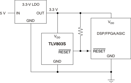
 Typical Application