SLVSES2J August   2018  – May 2021 TLV803E , TLV809E , TLV810E

PRODMIX  

  1. Features
  2. Applications
  3. Description
  4. Revision History
  5. Device Comparison
  6. Pin Configuration and Functions
  7. Specifications
    1. 7.1 Absolute Maximum Ratings
    2. 7.2 ESD Ratings
    3. 7.3 Recommended Operating Conditions
    4. 7.4 Thermal Information
    5. 7.5 Electrical Characteristics
    6. 7.6 Timing Requirements
    7. 7.7 Timing Diagrams
    8. 7.8 Typical Characteristics
  8. Detailed Description
    1. 8.1 Overview
    2. 8.2 Functional Block Diagram
    3. 8.3 Feature Description
      1. 8.3.1 Input Voltage (VDD)
      2. 8.3.2 VDD Hysteresis
      3. 8.3.3 VDD Glitch Immunity
      4. 8.3.4 Manual Reset (MR) Input for X2SON (DPW) Package Only
      5. 8.3.5 Output Logic
        1. 8.3.5.1 RESET Output, Active-Low
        2. 8.3.5.2 RESET Output, Active-High
    4. 8.4 Device Functional Modes
      1. 8.4.1 Normal Operation (VDD > VDD(min))
      2. 8.4.2 VDD Between VPOR and VDD(min)
      3. 8.4.3 Below Power-On-Reset (VDD < VPOR)
  9. Application and Implementation
    1. 9.1 Application Information
    2. 9.2 Typical Application - Voltage Rail Monitoring
      1. 9.2.1 Design Requirements
      2. 9.2.2 Detailed Design Procedure
      3. 9.2.3 Application Curves
    3. 9.3 Typical Application - Overvoltage Monitoring
      1. 9.3.1 Design Requirements
      2. 9.3.2 Detailed Design Procedure
  10. 10Power Supply Recommendations
  11. 11Layout
    1. 11.1 Layout Guidelines
    2. 11.2 Layout Example
  12. 12Device and Documentation Support
    1. 12.1 Device Support
      1. 12.1.1 Device Nomenclature
    2. 12.2 Documentation Support
      1. 12.2.1 Related Documentation
    3. 12.3 Receiving Notification of Documentation Updates
    4. 12.4 Support Resources
    5. 12.5 Trademarks
    6. 12.6 Electrostatic Discharge Caution
    7. 12.7 Glossary
  13. 13Mechanical, Packaging, and Orderable Information

Package Options

Mechanical Data (Package|Pins)
Thermal pad, mechanical data (Package|Pins)
Orderable Information

Manual Reset (MR) Input for X2SON (DPW) Package Only

The manual reset (MR) input allows a processor GPIO or other logic circuits to initiate a reset. A logic low on MR with pulse duration longer than tMR_RES will cause reset output to assert. After MR returns to a logic high
(VMR_H) and VDD is above VIT+, reset is deasserted after the user programmed reset time delay (tD) expires.

If MR is not controlled externally, then MR can be left disconnected. MR is internally connected to VDD through a pull-up resistor RMR shown in Section 8.2. If the logic signal controlling MR is less than VDD, then additional current flows from VDD into MR internally. For minimum current consumption, drive MR to either VDD or GND.
VMR should not be higher than VDD voltage.
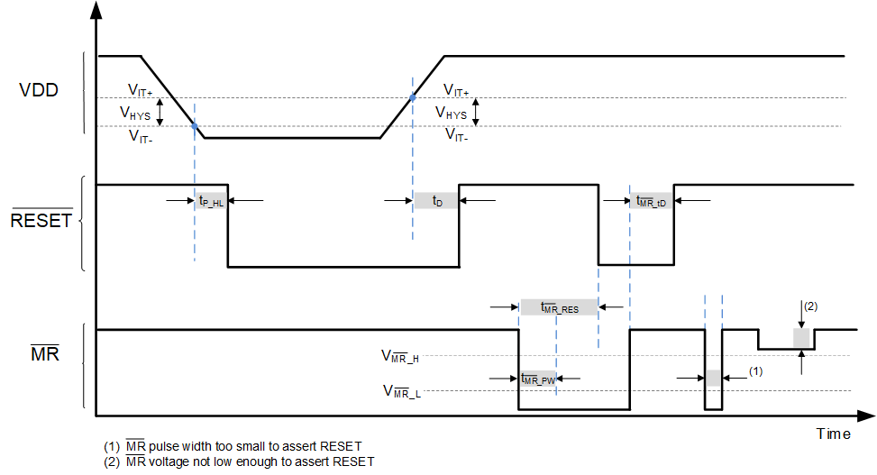
GUID-20200926-CA0I-XGHV-GMPS-P8R7LTMJDXHX-low.gif Figure 8-3 Timing Diagram MR and RESET for X2SON (DPW) Package