SLVSES2J August   2018  – May 2021 TLV803E , TLV809E , TLV810E

PRODMIX  

  1. Features
  2. Applications
  3. Description
  4. Revision History
  5. Device Comparison
  6. Pin Configuration and Functions
  7. Specifications
    1. 7.1 Absolute Maximum Ratings
    2. 7.2 ESD Ratings
    3. 7.3 Recommended Operating Conditions
    4. 7.4 Thermal Information
    5. 7.5 Electrical Characteristics
    6. 7.6 Timing Requirements
    7. 7.7 Timing Diagrams
    8. 7.8 Typical Characteristics
  8. Detailed Description
    1. 8.1 Overview
    2. 8.2 Functional Block Diagram
    3. 8.3 Feature Description
      1. 8.3.1 Input Voltage (VDD)
      2. 8.3.2 VDD Hysteresis
      3. 8.3.3 VDD Glitch Immunity
      4. 8.3.4 Manual Reset (MR) Input for X2SON (DPW) Package Only
      5. 8.3.5 Output Logic
        1. 8.3.5.1 RESET Output, Active-Low
        2. 8.3.5.2 RESET Output, Active-High
    4. 8.4 Device Functional Modes
      1. 8.4.1 Normal Operation (VDD > VDD(min))
      2. 8.4.2 VDD Between VPOR and VDD(min)
      3. 8.4.3 Below Power-On-Reset (VDD < VPOR)
  9. Application and Implementation
    1. 9.1 Application Information
    2. 9.2 Typical Application - Voltage Rail Monitoring
      1. 9.2.1 Design Requirements
      2. 9.2.2 Detailed Design Procedure
      3. 9.2.3 Application Curves
    3. 9.3 Typical Application - Overvoltage Monitoring
      1. 9.3.1 Design Requirements
      2. 9.3.2 Detailed Design Procedure
  10. 10Power Supply Recommendations
  11. 11Layout
    1. 11.1 Layout Guidelines
    2. 11.2 Layout Example
  12. 12Device and Documentation Support
    1. 12.1 Device Support
      1. 12.1.1 Device Nomenclature
    2. 12.2 Documentation Support
      1. 12.2.1 Related Documentation
    3. 12.3 Receiving Notification of Documentation Updates
    4. 12.4 Support Resources
    5. 12.5 Trademarks
    6. 12.6 Electrostatic Discharge Caution
    7. 12.7 Glossary
  13. 13Mechanical, Packaging, and Orderable Information

Package Options

Mechanical Data (Package|Pins)
Thermal pad, mechanical data (Package|Pins)
Orderable Information

Typical Application - Voltage Rail Monitoring

A typical application for TLV803E, TLV809E, and TLV810E devices is voltage rail monitoring. This rail can be the input power supply or the output of an LDO or DC/DC converter. Figure 9-1 shows the TLV803EA29 monitoring the supply rail for a DSP, FPGA, or ASIC. This rail is at 3.3 V and generated by an LDO with an input power supply of 5 V. The supervisor is needed to make sure that the supply to the MCU/ASIC/FPGA/DSP is above a certain voltage threshold. If the supply voltage drops below a certain threshold, supervisor generates a reset output to indicate to the MCU that the supply is going down so that the MCU can take actions to save register data before supply enters brown-out conditions.
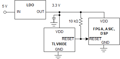
GUID-20200927-CA0I-FLHP-QQKN-B58PM2D33NXM-low.gif Figure 9-1 The Output of LDO Powering the MCU is Monitored by the TLV803EA29