SLVSES2J August 2018 – May 2021 TLV803E , TLV809E , TLV810E
PRODMIX
- 1 Features
- 2 Applications
- 3 Description
- 4 Revision History
- 5 Device Comparison
- 6 Pin Configuration and Functions
- 7 Specifications
- 8 Detailed Description
- 9 Application and Implementation
- 10Power Supply Recommendations
- 11Layout
- 12Device and Documentation Support
- 13Mechanical, Packaging, and Orderable Information
Package Options
Mechanical Data (Package|Pins)
Thermal pad, mechanical data (Package|Pins)
- DPW|5
Orderable Information
3 Description
The TLV803E, TLV809E, and TLV810E are enhanced alternatives to the TLV803, TLV853, TLV809, LM809, TPS3809 and TLV810. TLV80xE and TLV81xE offer low quiescent current IQ, higher accuracy, wider temperature range, and lower power-on-reset (VPOR) for increased system reliability.
The TLV80xE and TLV81xE family are low
IQ (250 nA typical, 1 µA max), voltage supervisory circuits (reset IC) that
monitor VDD voltage level. These devices initiate a reset signal whenever supply voltage VDD
drops below the factory programmed falling threshold voltage, VIT–. The reset
output remains low for a fixed reset time delay tD after the VDD voltage rises
above the rising voltage threshold (VIT+) which is equivalent to the falling
threshold voltage (VIT-) plus hysteresis
(VHYS).
These devices have integrated glitch immunity to ignore fast transients on the VDD pin. The low IQ and high accuracy (±0.5% typical) makes these voltage supervisors ideal for use in low-power and portable applications. The TLV80xE and TLV81xE devices are specified to have the defined output logic state for supply voltages down to VPOR = 0.7 V. The TLV80xE and TLV81xE devices are available in industry standard 3-pin SOT23 (DBZ) and SC70 (DCK) packages and very compact X2SON (DPW) package.
| PART NUMBER | PACKAGE | BODY SIZE (NOM) |
|---|---|---|
| TLV803E, TLV809E, TLV810E | SOT-23 (3) | 2.90 mm × 1.30 mm |
| SC-70 (3) | 2.00 mm × 1.25 mm | |
| X2SON (5) | 0.8 mm x 0.8 mm |
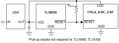
 Typical
Application