SLVSES2J August 2018 – May 2021 TLV803E , TLV809E , TLV810E
PRODMIX
- 1 Features
- 2 Applications
- 3 Description
- 4 Revision History
- 5 Device Comparison
- 6 Pin Configuration and Functions
- 7 Specifications
- 8 Detailed Description
- 9 Application and Implementation
- 10Power Supply Recommendations
- 11Layout
- 12Device and Documentation Support
- 13Mechanical, Packaging, and Orderable Information
Package Options
Mechanical Data (Package|Pins)
Thermal pad, mechanical data (Package|Pins)
- DPW|5
Orderable Information
7.8 Typical Characteristics
Typical characteristics show the typical
performance of the TLV803E, TLV809E, and TLV810E devices. Test conditions are
TA = 25°C, VDD = 3.3 V, VIT- = 2.93 V,
Rpull-up = 10 kΩ to 6 V, CLoad = 50 pF, unless otherwise noted.
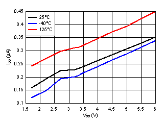 Figure 7-3 Supply Current Versus Supply Voltage for TLV803EA29
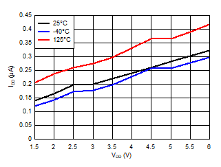 Figure 7-5 Supply Current Versus Supply Voltage for TLV810EA29
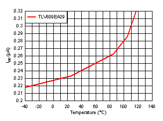 Figure 7-7 Supply Current Verses
Temperature for TLV809EA29, VDD = 3.3 V
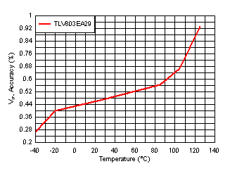 Figure 7-9 Voltage Threshold
Accuracy Verses Temperature for TLV803EA29
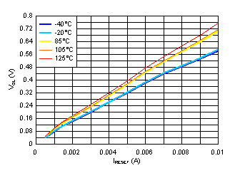 Figure 7-11 Low Voltage Output Versus Output Current for TLV803EA29, VDD = 1.7 V
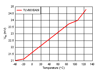 Figure 7-13 Low Voltage Output Verses
Temperature for TLV803EA29, VDD = 1.7 V
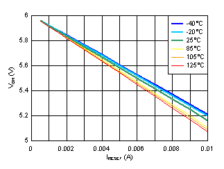 Figure 7-15 High Voltage Output Versus Output Current for TLV809EA29, VDD = 6 V
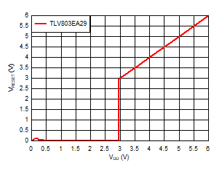 Figure 7-17 Reset Voltage Output Versus Voltage Input for TLV803EA29, Vpull-up = VDD, Rpull-up = 10 kΩ
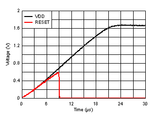 Figure 7-19 Transient Power-on-Reset Voltage for TLV809EA30, IRESET = 15 µA
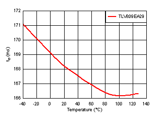 Figure 7-21 Reset Delay Time Verses
Temperature for TLV809EA29
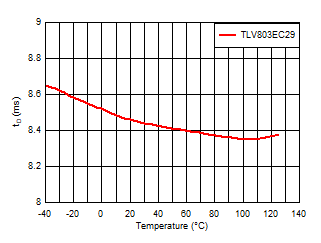 Figure 7-23 Reset Delay Time Verses
Temperature for TLV803EC29
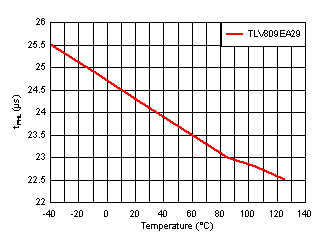 Figure 7-25 High-to-Low Propagation
Delay Verses Temperature for TLV809EA29
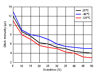 Figure 7-27 Glitch Immunity Versus Overdrive for TLV809EA29
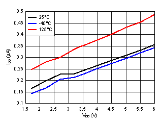 Figure 7-4 Supply Current Versus Supply Voltage for TLV809EA29
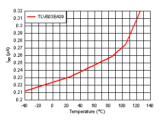 Figure 7-6 Supply Current Verses
Temperature for TLV803EA29, VDD = 3.3 V
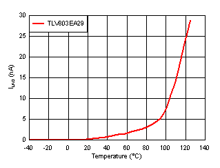 Figure 7-8 Leakage Current Verses
Temperature for TLV803EA29
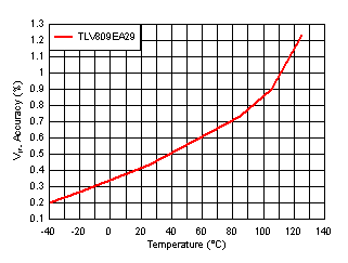 Figure 7-10 Voltage Threshold
Accuracy Verses Temperature for TLV809EA29
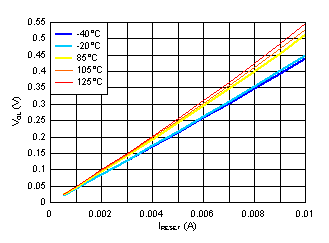 Figure 7-12 Low Voltage Output Versus Output Current for TLV809EA29, VDD = 1.7 V
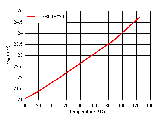 Figure 7-14 Low Voltage Output Verses
Temperature for TLV809EA29, VDD = 1.7 V
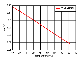 Figure 7-16 High Voltage Output
Verses Temperature for TLV809EA29, VDD = 3.3 V
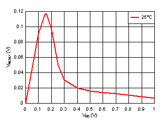 Figure 7-18 Reset Voltage Output Versus Voltage Input for TLV803EA29, Rpull-up = 10 kΩ
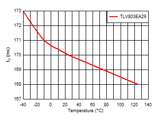 Figure 7-20 Reset Delay Time Verses
Temperature for TLV803EA29
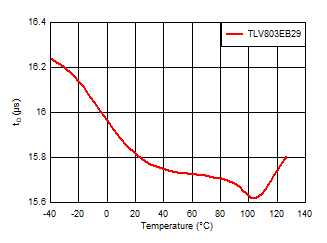 Figure 7-22 Reset Delay Time Verses
Temperature for TLV803EB29
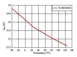 Figure 7-24 High-to-Low Propagation
Delay Verses Temperature for TLV803EA29
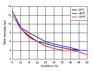 Figure 7-26 Glitch Immunity Versus Overdrive for TLV803EA29