SNVSBY3A November 2020 – April 2021 TLV840-Q1
PRODUCTION DATA
- 1 Features
- 2 Applications
- 3 Description
- 4 Revision History
- 5 Device Comparison
- 6 Pin Configuration and Functions
- 7 Specifications
- 8 Detailed Description
- 9 Application and Implementation
- 10Power Supply Recommendations
- 11Layout
- 12Device and Documentation Support
- 13Mechanical, Packaging, and Orderable Information
Package Options
Mechanical Data (Package|Pins)
- DBV|5
Thermal pad, mechanical data (Package|Pins)
Orderable Information
3 Description
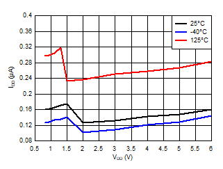
The TLV840-Q1 device is a voltage supervisor or reset IC that can operate at wide input voltage levels from 0.7 V to 6 V while maintaining very low quiescent current across the whole VDD and temperature range. TLV840-Q1 offers the best combination of low power consumption, high accuracy and low propagation delay (tp_HL= 30 µs typical).
Reset output signal is
asserted when the voltage at VDD drops below the negative voltage
threshold
(VIT-). Reset
signal is cleared when VDD rise above
VIT- plus hysteresis (VHYS) and the
reset time delay
(tD)
expires. Reset time delay can be programmed by connecting a
capacitor between the CT pin and ground. For a minimum reset delay
time the CT pin can be left floating. The TLV840-Q1, with its manual
reset pin (MR), offers program flexibility by
forcing the system into a hard reset when the pin is asserted.
Additional features: Low
power-on reset voltage
(VPOR), built-in glitch immunity protection for
VDD, built-in hysteresis, low open-drain output leakage current
(Ilkg(OD)). TLV840-Q1 is a perfect voltage
monitoring solution for automotive applications and battery-powered
/ low-power applications.
| PART NUMBER | PACKAGE (1) | BODY SIZE (NOM) |
|---|---|---|
| TLV840-Q1 | SOT-23 (5) (DBV) | 2.90 mm × 1.60 mm |
 Typical Application
Circuit
 Typical Supply
Current