SNOSD29E December 2016 – April 2018 TLV8541 , TLV8542 , TLV8544
UNLESS OTHERWISE NOTED, this document contains PRODUCTION DATA.
- 1 Features
- 2 Applications
- 3 Description
- 4 Revision History
- 5 Description (continued)
- 6 Pin Configuration and Functions
- 7 Specifications
- 8 Detailed Description
- 9 Application and Implementation
- 10Power Supply Recommendations
- 11Layout
- 12Device and Documentation Support
- 13Mechanical, Packaging, and Orderable Information
Package Options
Mechanical Data (Package|Pins)
Thermal pad, mechanical data (Package|Pins)
- RUG|8
Orderable Information
6 Pin Configuration and Functions
TLV8541 DBV Package
5-Pin SOT-23
Top View
Pin Functions: TLV8541 DBV
| PIN | I/O | DESCRIPTION | ||
|---|---|---|---|---|
| NUMBER | NAME | |||
| 1 | OUT | O | Output | |
| 2 | V– | P | Negative (lowest) power supply | |
| 3 | +IN | I | Non-Inverting Input | |
| 4 | –IN | I | Inverting Input | |
| 5 | V+ | P | Positive (highest) power supply | |
TLV8542 D Package
8-Pin SOIC
Top View
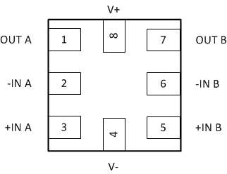
TLV8542 RUG Package
8-Pin X2QFN
Top View

Pin Functions: TLV8542 D & RUG
| PIN | I/O | DESCRIPTION | ||
|---|---|---|---|---|
| NUMBER | NAME | |||
| 1 | OUT A | O | Channel A Output | |
| 2 | –IN A | I | Channel A Inverting Input | |
| 3 | +IN A | I | Channel A Non-Inverting Input | |
| 4 | V– | P | Negative (lowest) power supply | |
| 5 | +IN B | I | Channel B Non-Inverting Input | |
| 6 | –IN B | I | Channel B Inverting Input | |
| 7 | OUT B | O | Channel B Output | |
| 8 | V+ | P | Positive (highest) power supply | |
TLV8544 PW and D Package
14-Pin TSSOP and SOIC
Top View
Pin Functions: TLV8544 PW & D
| PIN | I/O | DESCRIPTION | ||
|---|---|---|---|---|
| NUMBER | NAME | |||
| 1 | OUTA | O | Channel A output | |
| 2 | –INA | I | Channel A inverting input | |
| 3 | +INA | I | Channel A non-inverting input | |
| 4 | V+ | P | Positive (highest) power supply | |
| 5 | +INB | I | Channel B non-inverting input | |
| 6 | –INB | I | Channel B inverting input | |
| 7 | OUTB | O | Channel B output | |
| 8 | OUTC | O | Channel C output | |
| 9 | –INC | I | Channel C inverting input | |
| 10 | +INC | I | Channel C non-inverting input | |
| 11 | V– | P | Negative (lowest) power supply | |
| 12 | +IND | I | Channel D non-inverting input | |
| 13 | –IND | I | Channel D inverting input | |
| 14 | OUTD | O | Channel D output | |