SNOSD34A August 2016 – November 2016 TLV8801 , TLV8802
PRODUCTION DATA.
- 1 Features
- 2 Applications
- 3 Description
- 4 Revision History
- 5 Pin Configuration and Functions
- 6 Specifications
- 7 Detailed Description
- 8 Application and Implementation
- 9 Power Supply Recommendations
- 10Layout
- 11Device and Documentation Support
- 12Mechanical, Packaging, and Orderable Information
Package Options
Mechanical Data (Package|Pins)
- DGK|8
Thermal pad, mechanical data (Package|Pins)
Orderable Information
6 Specifications
6.1 Absolute Maximum Ratings
Over operating free-air temperature range (unless otherwise noted) (1)| MIN | MAX | UNIT | |||
|---|---|---|---|---|---|
| Supply voltage, Vs = (V+) - (V-) | –0.3 | 6 | V | ||
| Input pins | Voltage (2) (3) | Common mode | (V-) - 0.3 | (V+) + 0.3 | V |
| Differential | (V-) - 0.3 | (V+) + 0.3 | V | ||
| Input pins | Current | -10 | 10 | mA | |
| Output short current (4) | Continuous | Continuous | |||
| Storage temperature, Tstg | –65 | 150 | °C | ||
| Junction temperature | 150 | °C | |||
(1) Stresses beyond those listed under Absolute Maximum Ratings may cause permanent damage to the device. These are stress ratings only, which do not imply functional operation of the device at these or any other conditions beyond those indicated under Recommended Operating Conditions. Exposure to absolute-maximum-rated conditions for extended periods may affect device reliability.
(2) Not to exceed -0.3V or +6.0V on ANY pin, referred to V-
(3) Input terminals are diode-clamped to the power-supply rails. Input signals that can swing more than 0.3 V beyond the supply rails should be current-limited to 10 mA or less.
(4) Short-circuit to Vs/2, one amplifer per package. Continuous short circuit operation at elevated ambient temperature can result in exceeding the maximum allowed junction temperature of 150°C.
6.2 ESD Ratings
| VALUE | UNIT | |||
|---|---|---|---|---|
| V(ESD) | Electrostatic discharge | Human-body model (HBM), per ANSI/ESDA/JEDEC JS-001(1) | ±1000 | V |
| Charged-device model (CDM), per JEDEC specification JESD22-C101(2) | ±250 | |||
(1) JEDEC document JEP155 states that 500-V HBM allows safe manufacturing with a standard ESD control process. Manufacturing with less than 500-V HBM is possible with the necessary precautions. Pins listed as ±2000 V may actually have higher performance.
(2) JEDEC document JEP157 states that 250-V CDM allows safe manufacturing with a standard ESD control process. Manufacturing with less than 250-V CDM is possible with the necessary precautions. Pins listed as ±750 V may actually have higher performance.
6.3 Recommended Operating Conditions
over operating free-air temperature range (unless otherwise noted)| MIN | NOM | MAX | UNIT | ||
|---|---|---|---|---|---|
| Supply voltage (V+ – V–) | 1.7 | 5.5 | V | ||
| Specified temperature | -40 | 125 | °C | ||
6.4 Thermal Information
| THERMAL METRIC(1) | TLV8801 DBV 5 PINS | TLV8802 DGK 8 PINS | UNIT | |
|---|---|---|---|---|
| θJA | Junction-to-ambient thermal resistance | 177.4 | 177.6 | ºC/W |
| θJCtop | Junction-to-case (top) thermal resistance | 133.9 | 68.8 | |
| θJB | Junction-to-board thermal resistance | 36.3 | 98.2 | |
| ψJT | Junction-to-top characterization parameter | 23.6 | 12.3 | |
| ψJB | Junction-to-board characterization parameter | 35.7 | 96.7 | |
(1) For more information about traditional and new thermal metrics, see the Semiconductor and IC Package Thermal Metrics application report.
6.5 Electrical Characteristics
TA = 25°C, VS = 1.8V to 5 V, VCM = VOUT = VS/2, and RL≥ 10 MΩ to VS / 2, unless otherwise noted.6.6 Typical Characteristics
at TA = 25°C, RL = 10MΩ to VS/2 ,CL = 20pF, VCM = VS / 2V unless otherwise specified.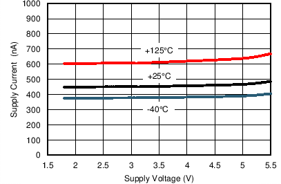
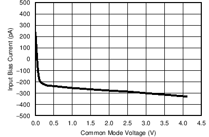
| VCM = V- | TLV8801 | RL=No Load |
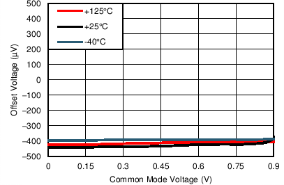
| VS= 1.8V | RL= 10MΩ |
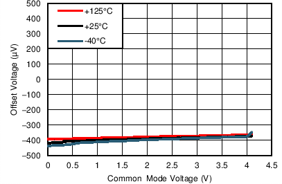
| VS= 5V | RL= 10MΩ |
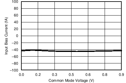
| VS= 1.8V | TA = -40°C |
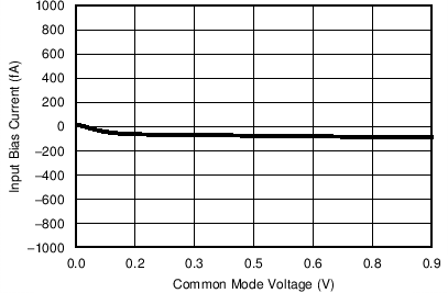
| VS= 1.8V | TA = 25°C |
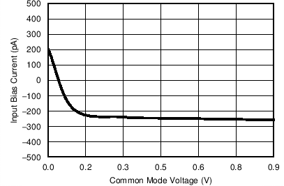
| VS= 1.8V | TA = 125°C |
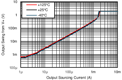
| VS= 1.8V | RL= No Load |
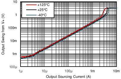
| VS= 3.3V | RL= No Load |
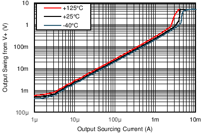
| VS= 5V | RL= No Load |

| TA = 25 | RL= 10MΩ | Vout = 200mVpp |
| VS= ±0.9V | CL= 20pF | AV = +1 |
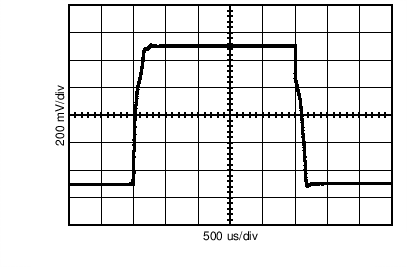
| TA = 25 | RL= 10MΩ | Vout = 1Vpp |
| VS= ±0.9V | CL= 20pF | AV = +1 |
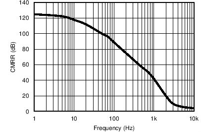
| TA = 25 | RL= 10MΩ | ΔVCM = 0.5Vpp |
| VS= 5V | CL= 20p | |
| VCM = Vs/2 | AV = +1 |
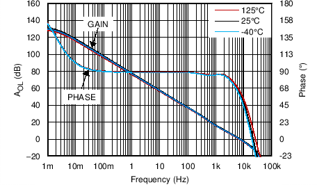
| TA = -40, 25, 125°C | RL= 10MΩ | VOUT = 200mVPP |
| VS= 5V | CL= 20pF | VCM = Vs/2 |

| TA = -40, 25, 125°C | RL= 1MΩ | VOUT = 200mVPP |
| VS= 5V | CL= 20pF | VCM = Vs/2 |
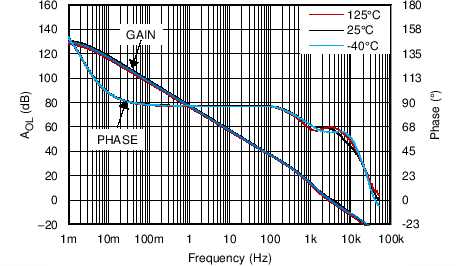
| TA = -40, 25, 125°C | RL= 100kΩ | VOUT = 200mVPP |
| VS= 5V | CL= 20pF | VCM = Vs/2 |
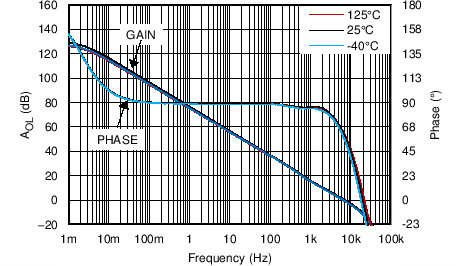
| TA = -40, 25, 125°C | RL= 10MΩ | VOUT = 200mVPP |
| VS= 1.8V | CL= 20pF | VCM = Vs/2 |

| TA = -40, 25, 125°C | RL= 1MΩ | VOUT = 200mVPP |
| VS= 1.8V | CL= 20pF | VCM = Vs/2 |
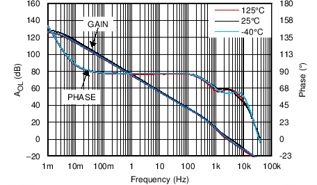
A.
Figure 35. Open Loop Gain and Phase, 1.8V, 100kΩ Load
| TA = -40, 25, 125°C | RL= 100kΩ | VOUT = 200mVPP |
| VS= 1.8V | CL= 20pF | VCM = Vs/2 |
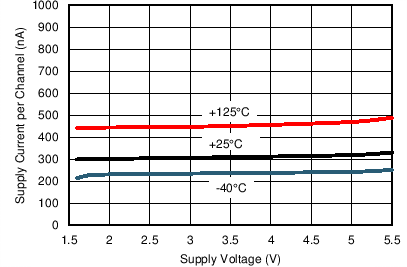
| VCM = V- | TLV8802 | RL=No Load |
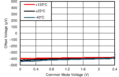
| VS= 3.3V | RL= 10MΩ |
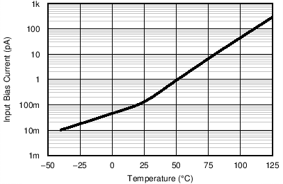
| VS= 5V | TA = -40 to 125 | VCM = Vs/2 |
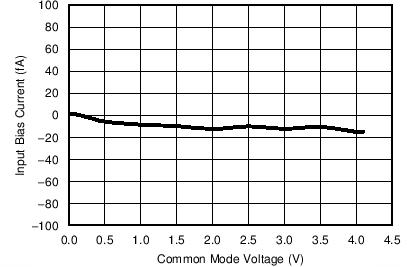
| VS= 5V | TA = -40°C |
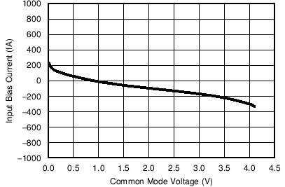
| VS= 5V | TA = 25°C |
| VS= 5V | TA = 125°C |
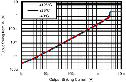
| VS= 1.8V | RL= No Load |
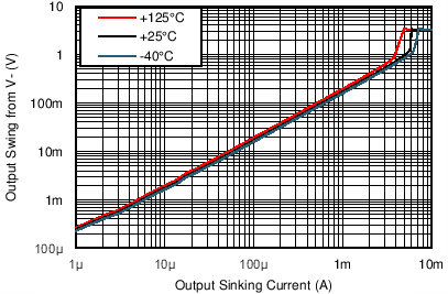
| VS= 3.3V | RL= No Load |
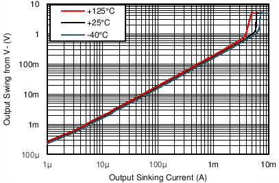
| VS= 5V | RL= No Load |
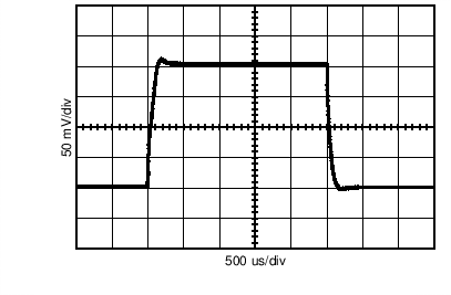
| TA = 25 | RL= 10MΩ | Vout = 200mVpp |
| VS= ±2.5V | CL= 20pF | AV = +1 |
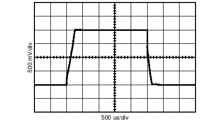
| TA = 25 | RL= 10MΩ | Vout = 2Vpp |
| VS= ±2.5V | CL= 20pF | AV = +1 |
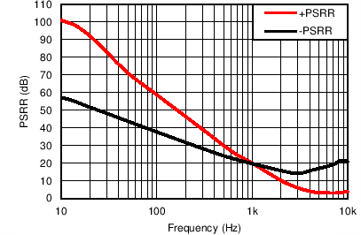
| TA = 25 | RL= 10MΩ | ΔVS = 0.5Vpp |
| VS= 3.3V | CL= 20p | |
| VCM = Vs/2 | AV = +1 |
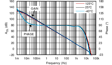
| TA = -40, 25, 125°C | RL= 10MΩ | VOUT = 200mVPP |
| VS= 3.3V | CL= 20pF | VCM = Vs/2 |
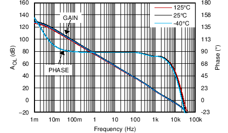
| TA = -40, 25, 125°C | RL= 1MΩ | VOUT = 200mVPP |
| VS= 3.3V | CL= 20pF | VCM = Vs/2 |
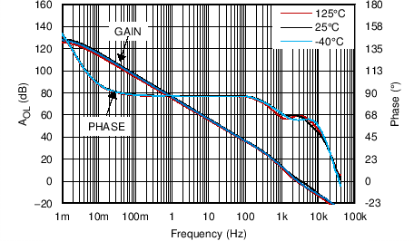
| TA = -40, 25, 125°C | RL= 100kΩ | VOUT = 200mVPP |
| VS= 3.3V | CL= 20pF | VCM = Vs/2 |
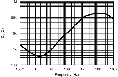
| TA = 25°C | VS= 5 V | RL= 10MΩ |
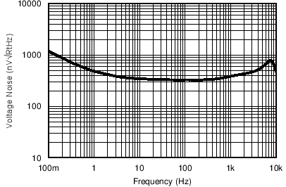
| TA = 25 | RL= 1MΩ | VCM = Vs/2 |
| VS= 5V | CL= 20pF | AV = +1 |
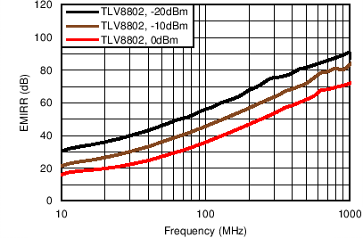
| TA = 25 | RL= 1MΩ | VCM = Vs/2 |
| VS= 3.3V | CL= 20pF | AV = +1 |