SBOS833R October 2017 – November 2021 TLV9001 , TLV9002 , TLV9004
PRODUCTION DATA
- 1 Features
- 2 Applications
- 3 Description
- 4 Revision History
- 5 Device Comparison Table
- 6 Pin Configuration and Functions
-
7 Specifications
- 7.1 Absolute Maximum Ratings
- 7.2 ESD Ratings
- 7.3 Recommended Operating Conditions
- 7.4 Thermal Information: TLV9001
- 7.5 Thermal Information: TLV9001S
- 7.6 Thermal Information: TLV9002
- 7.7 Thermal Information: TLV9002S
- 7.8 Thermal Information: TLV9004
- 7.9 Thermal Information: TLV9004S
- 7.10 Electrical Characteristics
- 7.11 Typical Characteristics
- 8 Detailed Description
- 9 Application and Implementation
- 10Power Supply Recommendations
- 11Layout
- 12Device and Documentation Support
- 13Mechanical, Packaging, and Orderable Information
Package Options
Refer to the PDF data sheet for device specific package drawings
Mechanical Data (Package|Pins)
- D|8
- DDF|8
- DGK|8
- DGS|10
- YCK|9
- PW|8
- RUG|10
- DSG|8
Thermal pad, mechanical data (Package|Pins)
Orderable Information
6 Pin Configuration and Functions
Figure 6-1 TLV9001 DBV, TLV9001T DCK Package
5-Pin SOT-23, SC70
Top View
5-Pin SOT-23, SC70
Top View
Figure 6-3 TLV9001 DPW Package
5-Pin X2SON
Top View
5-Pin X2SON
Top View
Figure 6-2 TLV9001 DCK Package, TLV9001 DRL Package,
TLV9001U DBV Package
5-Pin SC70, SOT-553, SOT-23
Top View
5-Pin SC70, SOT-553, SOT-23
Top View
Table 6-1 Pin Functions: TLV9001
| PIN | I/O | DESCRIPTION | |||
|---|---|---|---|---|---|
| NAME | SOT-23, SC70(T) |
SC70, SOT-23(U), SOT-553 |
X2SON | ||
| IN– | 4 | 3 | 2 | I | Inverting input |
| IN+ | 3 | 1 | 4 | I | Noninverting input |
| OUT | 1 | 4 | 1 | O | Output |
| V– | 2 | 2 | 3 | I or — | Negative (low) supply or ground (for single-supply operation) |
| V+ | 5 | 5 | 5 | I | Positive (high) supply |
Figure 6-4 TLV9001S DBV Package
6-Pin SOT-23
Top View
6-Pin SOT-23
Top View
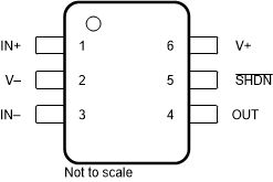
 Figure 6-5 TLV9001S DCK Package
6-Pin SC70
Top View
Table 6-2 Pin Functions: TLV9001S
| PIN | I/O | DESCRIPTION | ||
|---|---|---|---|---|
| NAME | SOT-23 | SC70 | ||
| IN– | 4 | 3 | I | Inverting input |
| IN+ | 3 | 1 | I | Noninverting input |
| OUT | 1 | 4 | O | Output |
| SHDN | 5 | 5 | I | Shutdown: low = amp disabled, high = amp enabled. See Section 8.5 for more information. |
| V– | 2 | 2 | I or — | Negative (low) supply or ground (for single-supply operation) |
| V+ | 6 | 6 | I | Positive (high) supply |
Figure 6-6 TLV9002 D, DGK, PW, DDF Package
8-Pin SOIC, VSSOP, TSSOP, SOT-23
Top View
8-Pin SOIC, VSSOP, TSSOP, SOT-23
Top View
Connect thermal pad to
V–.
Figure 6-7 TLV9002 DSG Package8-Pin WSON With Exposed Thermal Pad
Top View
Table 6-3 Pin Functions: TLV9002
| PIN | I/O | DESCRIPTION | ||
|---|---|---|---|---|
| NAME | NO. | |||
| IN1– | 2 | I | Inverting input, channel 1 | |
| IN1+ | 3 | I | Noninverting input, channel 1 | |
| IN2– | 6 | I | Inverting input, channel 2 | |
| IN2+ | 5 | I | Noninverting input, channel 2 | |
| OUT1 | 1 | O | Output, channel 1 | |
| OUT2 | 7 | O | Output, channel 2 | |
| V– | 4 | I or — | Negative (low) supply or ground (for single-supply operation) | |
| V+ | 8 | I | Positive (high) supply | |
Figure 6-8 TLV9002S DGS Package
10-Pin VSSOP
Top View
10-Pin VSSOP
Top View
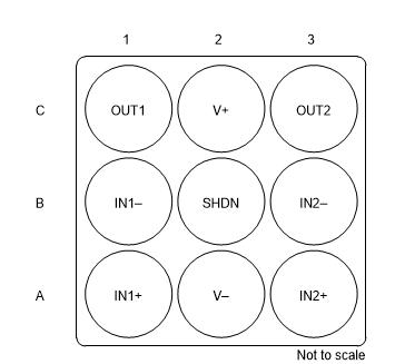
 Figure 6-10 TLV9002S YCK Package
9-Pin DSBGA (WCSP)
Bottom View
Figure 6-9 TLV9002S RUG Package
10-Pin X2QFN
Top View
10-Pin X2QFN
Top View
Table 6-4 Pin Functions: TLV9002S
| PIN | I/O | DESCRIPTION | |||
|---|---|---|---|---|---|
| NAME | VSSOP | X2QFN | DSBGA (WCSP) | ||
| IN1– | 2 | 9 | B1 | I | Inverting input, channel 1 |
| IN1+ | 3 | 10 | A1 | I | Noninverting input, channel 1 |
| IN2– | 8 | 5 | B3 | I | Inverting input, channel 2 |
| IN2+ | 7 | 4 | A3 | I | Noninverting input, channel 2 |
| OUT1 | 1 | 8 | C1 | O | Output, channel 1 |
| OUT2 | 9 | 6 | C3 | O | Output, channel 2 |
| SHDN1 | 5 | 2 | — | I | Shutdown: low = amp disabled, high = amp enabled, channel 1. See Section 8.5 for more information. |
| SHDN2 | 6 | 3 | — | I | Shutdown: low = amp disabled, high = amp enabled, channel 1. See Section 8.5 for more information. |
| SHDN | — | — | B2 | Shutdown: low = both amplifiers disabled, high = both amplifiers enabled | |
| V– | 4 | 1 | A2 | I or — | Negative (low) supply or ground (for single-supply operation) |
| V+ | 10 | 7 | C2 | I | Positive (high) supply |
Figure 6-11 TLV9004 D, DYY, PW Package
14-Pin SOIC, SOT-23 (14), TSSOP
Top View
14-Pin SOIC, SOT-23 (14), TSSOP
Top View
Connect thermal pad to
V–.
Figure 6-13 TLV9004 RTE Package16-Pin WQFN With Exposed Thermal Pad
Top View
Figure 6-12 TLV9004 RUC Package
14-Pin X2QFN
Top View
14-Pin X2QFN
Top View
Table 6-5 Pin Functions: TLV9004
| PIN | I/O | DESCRIPTION | |||
|---|---|---|---|---|---|
| NAME | SOIC, SOT-23 (14), TSSOP | WQFN | X2QFN | ||
| IN1– | 2 | 16 | 1 | I | Inverting input, channel 1 |
| IN1+ | 3 | 1 | 2 | I | Noninverting input, channel 1 |
| IN2– | 6 | 4 | 5 | I | Inverting input, channel 2 |
| IN2+ | 5 | 3 | 4 | I | Noninverting input, channel 2 |
| IN3– | 9 | 9 | 8 | I | Inverting input, channel 3 |
| IN3+ | 10 | 10 | 9 | I | Noninverting input, channel 3 |
| IN4– | 13 | 13 | 12 | I | Inverting input, channel 4 |
| IN4+ | 12 | 12 | 11 | I | Noninverting input, channel 4 |
| NC | — | 6, 7 | — | — | No internal connection |
| OUT1 | 1 | 15 | 14 | O | Output, channel 1 |
| OUT2 | 7 | 5 | 6 | O | Output, channel 2 |
| OUT3 | 8 | 8 | 7 | O | Output, channel 3 |
| OUT4 | 14 | 14 | 13 | O | Output, channel 4 |
| V– | 11 | 11 | 10 | I or — | Negative (low) supply or ground (for single-supply operation) |
| V+ | 4 | 2 | 3 | I | Positive (high) supply |
Connect thermal pad to V–.
Figure 6-14 TLV9004S RTE Package16-Pin WQFN With Exposed Thermal Pad
Top View
Table 6-6 Pin Functions: TLV9004S
| PIN | I/O | DESCRIPTION | |
|---|---|---|---|
| NAME | NO. | ||
| IN1+ | 1 | I | Noninverting input |
| IN1– | 16 | I | Inverting input |
| IN2+ | 3 | I | Noninverting input |
| IN2– | 4 | I | Inverting input |
| IN3+ | 10 | I | Noninverting input |
| IN3– | 9 | I | Inverting input |
| IN4+ | 12 | I | Noninverting input |
| IN4– | 13 | I | Inverting input |
| SHDN12 | 6 | I | Shutdown: low = amp disabled, high = amp enabled, channel 1 and 2. See Section 8.5 for more information. |
| SHDN34 | 7 | I | Shutdown: low = amp disabled, high = amp enabled, channel 3 and 4. See Section 8.5 for more information. |
| OUT1 | 15 | O | Output |
| OUT2 | 5 | O | Output |
| OUT3 | 8 | O | Output |
| OUT4 | 14 | O | Output |
| V– | 11 | I or — | Negative (low) supply or ground (for single-supply operation) |
| V+ | 2 | I | Positive (high) supply |