SBOS942J August 2018 – February 2024 TLV9051 , TLV9052 , TLV9054
PRODUCTION DATA
- 1
- 1 Features
- 2 Applications
- 3 Description
- 4 Device Comparison Table
- 5 Pin Configuration and Functions
-
6 Specifications
- 6.1 Absolute Maximum Ratings
- 6.2 ESD Ratings
- 6.3 Recommended Operating Conditions
- 6.4 Thermal Information for Single Channel
- 6.5 Thermal Information for Dual Channel
- 6.6 Thermal Information for Quad Channel
- 6.7 Electrical Characteristics: VS (Total Supply Voltage) = (V+) – (V–) = 1.8 V to 5.5 V
- 6.8 Typical Characteristics
- 7 Detailed Description
- 8 Application and Implementation
- 9 Device and Documentation Support
- 10Revision History
- 11Mechanical, Packaging, and Orderable Information
7.3.8 Input Protection
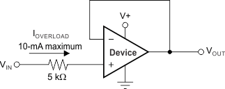
The TLV905x family incorporates internal ESD protection circuits on all pins. For input and output pins, this protection primarily consists of current-steering diodes connected between the input and power-supply pins. These ESD protection diodes provide in-circuit, input overdrive protection, as long as the current is limited to 10mA, as shown in the Section 6.1. Figure 7-3 shows how a series input resistor can be added to the driven input to limit the input current. The added resistor contributes thermal noise at the amplifier input and the value must be kept to a minimum in noise-sensitive applications.
 Figure 7-3 Input Current Protection