SBOS943E February 2019 – August 2021 TLV9101 , TLV9102 , TLV9104
PRODUCTION DATA
- 1 Features
- 2 Applications
- 3 Description
- 4 Revision History
- 5 Pin Configuration and Functions
- 6 Specifications
-
7 Detailed Description
- 7.1 Overview
- 7.2 Functional Block Diagram
- 7.3
Feature Description
- 7.3.1 EMI Rejection
- 7.3.2 Phase Reversal Protection
- 7.3.3 Thermal Protection
- 7.3.4 Capacitive Load and Stability
- 7.3.5 Common-Mode Voltage Range
- 7.3.6 Electrical Overstress
- 7.3.7 Overload Recovery
- 7.3.8 Typical Specifications and Distributions
- 7.3.9 Packages With an Exposed Thermal Pad
- 7.3.10 Shutdown
- 7.4 Device Functional Modes
- 8 Application and Implementation
- 9 Power Supply Recommendations
- 10Layout
- 11Device and Documentation Support
- 12Mechanical, Packaging, and Orderable Information
Package Options
Mechanical Data (Package|Pins)
Thermal pad, mechanical data (Package|Pins)
Orderable Information
7.3.1 EMI Rejection
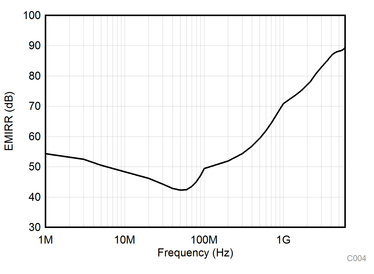
The TLV910x uses integrated electromagnetic interference (EMI) filtering to reduce the effects of EMI from sources such as wireless communications and densely-populated boards with a mix of analog signal chain and digital components. EMI immunity can be improved with circuit design techniques; the TLV910x benefits from these design improvements. Texas Instruments has developed the ability to accurately measure and quantify the immunity of an operational amplifier over a broad frequency spectrum extending from 10 MHz to 6 GHz. Figure 7-1 shows the results of this testing on the TLV910x. Table 7-1 shows the EMIRR IN+ values for the TLV910x at particular frequencies commonly encountered in real-world applications. Table 7-1 lists applications that can be centered on or operated near the particular frequency shown. The EMI Rejection Ratio of Operational Amplifiers application report contains detailed information on the topic of EMIRR performance as it relates to op amps and is available for download from www.ti.com.
 Figure 7-1 TLV910x EMIRR Testing
| FREQUENCY | APPLICATION OR ALLOCATION | EMIRR IN+ |
|---|---|---|
| 400 MHz | Mobile radio, mobile satellite, space operation, weather, radar, ultra-high frequency (UHF) applications | 59.5 dB |
| 900 MHz | Global system for mobile communications (GSM) applications, radio communication, navigation, GPS (to 1.6 GHz), GSM, aeronautical mobile, UHF applications | 68.9 dB |
| 1.8 GHz | GSM applications, mobile personal communications, broadband, satellite, L-band (1 GHz to 2 GHz) | 77.8 dB |
| 2.4 GHz | 802.11b, 802.11g, 802.11n, Bluetooth®, mobile personal communications, industrial, scientific and medical (ISM) radio band, amateur radio and satellite, S-band (2 GHz to 4 GHz) | 78.0 dB |
| 3.6 GHz | Radiolocation, aero communication and navigation, satellite, mobile, S-band | 88.8 dB |
| 5 GHz | 802.11a, 802.11n, aero communication and navigation, mobile communication, space and satellite operation, C-band (4 GHz to 8 GHz) | 87.6 dB |