SBOS943E February 2019 – August 2021 TLV9101 , TLV9102 , TLV9104
PRODUCTION DATA
- 1 Features
- 2 Applications
- 3 Description
- 4 Revision History
- 5 Pin Configuration and Functions
- 6 Specifications
-
7 Detailed Description
- 7.1 Overview
- 7.2 Functional Block Diagram
- 7.3
Feature Description
- 7.3.1 EMI Rejection
- 7.3.2 Phase Reversal Protection
- 7.3.3 Thermal Protection
- 7.3.4 Capacitive Load and Stability
- 7.3.5 Common-Mode Voltage Range
- 7.3.6 Electrical Overstress
- 7.3.7 Overload Recovery
- 7.3.8 Typical Specifications and Distributions
- 7.3.9 Packages With an Exposed Thermal Pad
- 7.3.10 Shutdown
- 7.4 Device Functional Modes
- 8 Application and Implementation
- 9 Power Supply Recommendations
- 10Layout
- 11Device and Documentation Support
- 12Mechanical, Packaging, and Orderable Information
Package Options
Mechanical Data (Package|Pins)
Thermal pad, mechanical data (Package|Pins)
Orderable Information
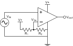
8.2.1 High Voltage Precision Comparator
Many different systems require controlled voltages across numerous system nodes to ensure robust operation. A comparator can be used to monitor and control voltages by comparing a reference threshold voltage with an input voltage and providing an output when the input crosses this threshold.
The TLV910x family of op amps make excellent high voltage, precision comparators due to their robust input stage, low typical offset, and high slew rate. Previous generation high-voltage op amps often use back-to-back diodes across the inputs to prevent damage to the op amp which greatly limits these op amps to be used as comparators, but the patented input stage of the TLV910x allows the device to have a wide differential voltage between the inputs.
 Figure 8-1 Typical Comparator Application