SBOSA23G May 2020 – March 2024 TLV9151-Q1 , TLV9152-Q1 , TLV9154-Q1
PRODUCTION DATA
- 1
- 1 Features
- 2 Applications
- 3 Description
- 4 Pin Configuration and Functions
- 5 Specifications
- 6 Detailed Description
- 7 Application and Implementation
- 8 Device and Documentation Support
- 9 Revision History
- 10Mechanical, Packaging, and Orderable Information
Package Options
Mechanical Data (Package|Pins)
Thermal pad, mechanical data (Package|Pins)
Orderable Information
4 Pin Configuration and Functions
 Figure 4-1 TLV9151-Q1 DBV Package,
5-Pin SOT-23
(Top View)
 Figure 4-2 TLV9151-Q1 DCK Package,
5-Pin SC70
(Top View)
Table 4-1 Pin Functions: TLV9151-Q1
| PIN | TYPE(1) | DESCRIPTION | ||
|---|---|---|---|---|
| NAME | DBV | DCK | ||
| IN+ | 3 | 1 | I | Noninverting input |
| IN– | 4 | 3 | I | Inverting input |
| OUT | 1 | 4 | O | Output |
| V+ | 5 | 5 | — | Positive (highest) power supply |
| V– | 2 | 2 | — | Negative (lowest) power supply |
(1) I = input, O = output
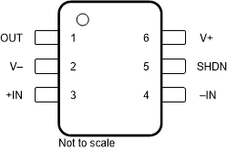
 Figure 4-3 TLV9151S-Q1 DBV Package,
6-Pin SOT-23
(Top View)
Table 4-2 Pin Functions: TLV9151S-Q1
| PIN | TYPE1 | DESCRIPTION | |
|---|---|---|---|
| NAME | NO. | ||
| IN+ | 3 | I | Noninverting input |
| IN– | 4 | I | Inverting input |
| OUT | 1 | O | Output |
| SHDN | 5 | I | Shutdown: low = amplifier enabled, high = amplifier disabled. See Section 6.3.9 for more information. |
| V+ | 6 | — | Positive (highest) power supply |
| V– | 2 | — | Negative (lowest) power supply |
- I = input, O = output
 Figure 4-4 TLV9152-Q1 D, PW and DGK Package,
8-Pin SOIC, TSSOP and VSSOP
(Top View)
Table 4-3 Pin Functions: TLV9152-Q1
| PIN | TYPE(1) | DESCRIPTION | |
|---|---|---|---|
| NAME | NO. | ||
| IN1+ | 3 | I | Noninverting input, channel 1 |
| IN2+ | 5 | I | Noninverting input, channel 2 |
| IN1– | 2 | I | Inverting input, channel 1 |
| IN2– | 6 | I | Inverting input, channel 2 |
| OUT1 | 1 | O | Output, channel 1 |
| OUT2 | 7 | O | Output, channel 2 |
| V+ | 8 | — | Positive (highest) power supply |
| V– | 4 | — | Negative (lowest) power supply |
(1) I = input, O = output
 Figure 4-5 TLV9154-Q1 D, DYY, and PW Package,
14-Pin SOIC, SOT-23, and TSSOP
(Top View)
Table 4-4 Pin Functions: TLV9154-Q1
| PIN | TYPE(1) | DESCRIPTION | |
|---|---|---|---|
| NAME | NO. | ||
| IN1+ | 3 | I | Noninverting input, channel 1 |
| IN1– | 2 | I | Inverting input, channel 1 |
| IN2+ | 5 | I | Noninverting input, channel 2 |
| IN2– | 6 | I | Inverting input, channel 2 |
| IN3+ | 10 | I | Noninverting input, channel 3 |
| IN3– | 9 | I | Inverting input, channel 3 |
| IN4+ | 12 | I | Noninverting input, channel 4 |
| IN4– | 13 | I | Inverting input, channel 4 |
| OUT1 | 1 | O | Output, channel 1 |
| OUT2 | 7 | O | Output, channel 2 |
| OUT3 | 8 | O | Output, channel 3 |
| OUT4 | 14 | O | Output, channel 4 |
| V+ | 4 | — | Positive (highest) power supply |
| V– | 11 | — | Negative (lowest) power supply |
(1) I = input, O = output