SBOSA67B November   2021  – March 2022 TLV9361 , TLV9362 , TLV9364

PRODUCTION DATA  

  1. Features
  2. Applications
  3. Description
  4. Revision History
  5. Pin Configuration and Functions
  6. Specifications
    1. 6.1 Absolute Maximum Ratings
    2. 6.2 ESD Ratings
    3. 6.3 Recommended Operating Conditions
    4. 6.4 Thermal Information for Single Channel
    5. 6.5 Thermal Information for Dual Channel
    6. 6.6 Thermal Information for Quad Channel
    7. 6.7 Electrical Characteristics
    8. 6.8 Typical Characteristics
  7. Detailed Description
    1. 7.1 Overview
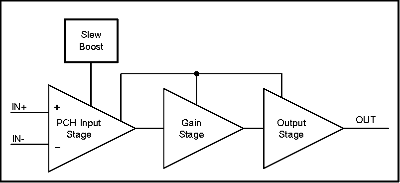
    2. 7.2 Functional Block Diagram
    3. 7.3 Feature Description
      1. 7.3.1 EMI Rejection
      2. 7.3.2 Thermal Protection
      3. 7.3.3 Capacitive Load and Stability
      4. 7.3.4 Electrical Overstress
      5. 7.3.5 Overload Recovery
      6. 7.3.6 Typical Specifications and Distributions
    4. 7.4 Device Functional Modes
  8. Application Information Disclaimer
    1. 8.1 Application Information
    2. 8.2 Typical Applications
      1. 8.2.1 Unity-Gain Buffer With RISO Stability Compensation
        1. 8.2.1.1 Design Requirements
        2. 8.2.1.2 Detailed Design Procedure
        3. 8.2.1.3 Application Curve
  9. Power Supply Recommendations
  10. 10Layout
    1. 10.1 Layout Guidelines
    2. 10.2 Layout Example
  11. 11Device and Documentation Support
    1. 11.1 Device Support
      1. 11.1.1 Development Support
        1. 11.1.1.1 TINA-TI (Free Software Download)
        2. 11.1.1.2 TI Precision Designs
    2. 11.2 Documentation Support
      1. 11.2.1 Related Documentation
    3. 11.3 Receiving Notification of Documentation Updates
    4. 11.4 Support Resources
    5. 11.5 Trademarks
    6. 11.6 Electrostatic Discharge Caution
    7. 11.7 Glossary
  12. 12Mechanical, Packaging, and Orderable Information

Package Options

Mechanical Data (Package|Pins)
Thermal pad, mechanical data (Package|Pins)
Orderable Information

Functional Block Diagram

GUID-20210820-SS0I-DMPZ-K7MN-CFDCDN475ZB4-low.png