SBOSA67B November 2021 – March 2022 TLV9361 , TLV9362 , TLV9364
PRODUCTION DATA
- 1 Features
- 2 Applications
- 3 Description
- 4 Revision History
- 5 Pin Configuration and Functions
- 6 Specifications
- 7 Detailed Description
- 8 Application Information Disclaimer
- 9 Power Supply Recommendations
- 10Layout
- 11Device and Documentation Support
- 12Mechanical, Packaging, and Orderable Information
Package Options
Mechanical Data (Package|Pins)
Thermal pad, mechanical data (Package|Pins)
- DGK|8
Orderable Information
8.2.1.2 Detailed Design Procedure
Figure 8-1 shows a unity-gain buffer driving a capacitive load. Equation 1 shows the transfer function for the circuit in Figure 8-1. Figure 8-1 does not show the open-loop output resistance of the operational amplifier (Ro).
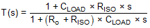
The transfer function in Equation 1 has a pole and a zero. The frequency of the pole (fp) is determined by (Ro + RISO) and CLOAD. The RISO and CLOAD components determine the frequency of the zero (fz). A stable system is obtained by selecting RISO so that the rate of closure (ROC) between the open-loop gain (AOL) and 1/β is 20 dB per decade. Figure 8-2 shows the concept. The 1/β curve for a unity-gain buffer is 0 dB.
 Figure 8-2 Unity-Gain Amplifier With RISO Compensation
Typically, ROC stability analysis is simulated. The validity of the analysis depends on multiple factors, especially the accurate modeling of Ro. In addition to simulating the ROC, a robust stability analysis includes a measurement of overshoot percentage and/or AC gain peaking of the circuit using a function generator, oscilloscope, and gain and phase analyzer. Phase margin is then calculated from these measurements. Table 8-1 shows the overshoot percentage and AC gain peaking that correspond to a phase margin of 45°. For more details on this design and other alternative devices that can replace the TLV936x, see the Capacitive Load Drive Solution Using an Isolation Resistor precision design.
| PHASE MARGIN | OVERSHOOT | AC GAIN PEAKING |
|---|---|---|
| 45° | 23.3% | 2.35 dB |