SBAS933D December 2020 – June 2022 TMAG5110 , TMAG5111
PRODUCTION DATA
- 1 Features
- 2 Applications
- 3 Description
- 4 Revision History
- 5 Device Comparison
- 6 Pin Configuration and Functions
- 7 Specifications
- 8 Detailed Description
- 9 Application and Implementation
- 10Power Supply Recommendations
- 11Layout
- 12Device and Documentation Support
- 13Mechanical, Packaging, and Orderable Information
Package Options
Refer to the PDF data sheet for device specific package drawings
Mechanical Data (Package|Pins)
- DBV|5
Thermal pad, mechanical data (Package|Pins)
Orderable Information
8.3.6 Power Derating
The device is specified from –40 °C to 125 °C for a voltage rating of 2.5 V to 38 V. Because the part is draining at its maximum a current of 17 mA the maximum voltage that can be applied will depend on what is the maximum ambient temperature acceptable for the application. The curve in Figure 8-22 shows the maximum acceptable power supply voltage versus the maximum acceptable ambient temperature.
The Figure 8-22 can also be calculated using the following formulas:
where
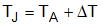
- TJ is the junction temperature
- TA is the ambient temperature
- ΔT is the difference between the junction temperature and the ambient temperature
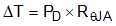
where
- PD is the power dissipated by the part
- RθJA is the junction to ambient thermal resistance
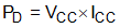
where
- VCC is the voltage supply of the device
- ICC is the current consumption of the device
Combining the three equations above gives Equation 4 below:
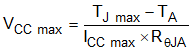
This equation gives the maximum voltage the part can handle in regards of the ambient temperature.
For example, in the application required to work within a ambient temperature of maximum 85 °C, with TJmax, RθJA and ICCmax are defined in the data sheet, the maximum voltage allowed for this application is determined in Equation 5:
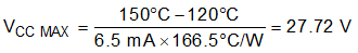
 Figure 8-22 Power Derating Curve