SBAS933D December 2020 – June 2022 TMAG5110 , TMAG5111
PRODUCTION DATA
- 1 Features
- 2 Applications
- 3 Description
- 4 Revision History
- 5 Device Comparison
- 6 Pin Configuration and Functions
- 7 Specifications
- 8 Detailed Description
- 9 Application and Implementation
- 10Power Supply Recommendations
- 11Layout
- 12Device and Documentation Support
- 13Mechanical, Packaging, and Orderable Information
Package Options
Refer to the PDF data sheet for device specific package drawings
Mechanical Data (Package|Pins)
- DBV|5
Thermal pad, mechanical data (Package|Pins)
Orderable Information
8.3.3 Power-On Time
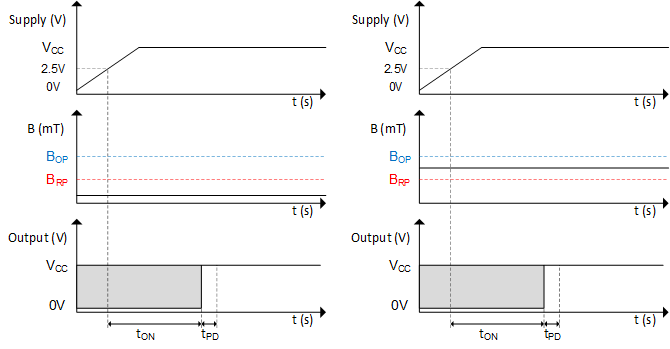
Figure 8-17 shows the behavior of the device after the VCC voltage is applied and when the field is below the BOP threshold. Once the minimum value for VCC is reached, the TMAG5110 will take time tON to power up and then time tPD to update the output to a level High.
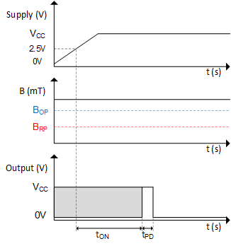
Figure 8-18 shows the behavior of the device after the VCC voltage is applied and when the field is above the BOP threshold. Once the minimum value for VCC is reached, the TMAG5110 will take time tON to power up and then time tPD to update the output to a level High.
For the TMAG5111 the power-on behavior is similar but OUT1 will be updated to Low during the tPD time. OUT2 will be updated to High during the tPD time. The output value following the power-on sequence will then depend on the magnet placement, the sense of rotation and the device variant.
 Figure 8-17 Power-On Time When
B<BOP
 Figure 8-18 Power-On Time When
B>BOP