SBOSA72 July 2021 TMCS1108-Q1
PRODUCTION DATA
- 1 Features
- 2 Applications
- 3 Description
- 4 Revision History
- 5 Device Comparison
- 6 Pin Configuration and Functions
- 7 Specifications
- 8 Parameter Measurement Information
- 9 Detailed Description
- 10Application and Implementation
- 11Power Supply Recommendations
- 12Layout
- 13Device and Documentation Support
- 14Mechanical, Packaging, and Orderable Information
Package Options
Refer to the PDF data sheet for device specific package drawings
Mechanical Data (Package|Pins)
- D|8
Thermal pad, mechanical data (Package|Pins)
Orderable Information
9.3.2.1 Lifetime and Environmental Stability
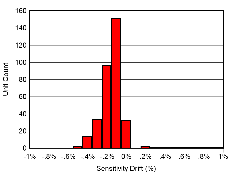
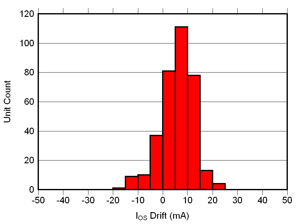
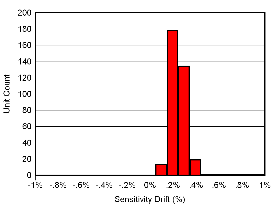
The same compensation techniques utilized in the TMCS1108-Q1 to reduce temperature drift also greatly reduce lifetime drift due to aging, stress, and environmental conditions. Typical magnetic sensors suffer from up to 2% to 3% of sensitivity drift due to aging at high operating temperatures. The TMCS1108-Q1 has greatly improved lifetime drift, as defined in the Electrical Characteristics table for total sensitivity error measured after the worst-case stress test during a three lot AEC-Q100 qualification. All other stress tests prescribed by an AEC-Q100 qualification caused lower than the specified sensitivity error, and were within the bounds specified within the Electrical Characteristics table. Figure 9-1 shows the total sensitivity error after the worst case stress test, a Highly Accelerated Stress Test (HAST) at 130°C and 85% relative humidity (RH), while Figure 9-2 and Figure 9-3 show the sensitivity and offset error drift after a 1000 hour, 125°C high temperature operating life stress test as specified by AEC-Q100. This test mimics typical device lifetime operation, and shows the likely device performance variation due to aging is vastly improved compared to typical magnetic sensors.
 Figure 9-1 Sensitivity Error After
130°C, 85% RH HAST
 Figure 9-3 Input-Referred Offset
Drift After AEC-Q100 High Temperature Operating Life Stress Test
 Figure 9-2 Sensitivity Error Drift
After AEC-Q100 High Temperature Operating Life Stress Test