SBOS397H August 2007 – December 2018 TMP102
PRODUCTION DATA.
- 1 Features
- 2 Applications
- 3 Description
- 4 Revision History
- 5 Pin Configuration and Functions
- 6 Specifications
-
7 Detailed Description
- 7.1 Overview
- 7.2 Functional Block Diagram
- 7.3 Feature Description
- 7.4 Device Functional Modes
- 7.5
Programming
- 7.5.1 Pointer Register
- 7.5.2 Temperature Register
- 7.5.3
Configuration Register
- Table 10. Byte 1 of Configuration and Power-Up or Reset Format
- Table 11. Byte 2 of Configuration and Power-Up or Reset Format
- 7.5.3.1 Shutdown Mode (SD)
- 7.5.3.2 Thermostat Mode (TM)
- 7.5.3.3 Polarity (POL)
- 7.5.3.4 Fault Queue (F1/F0)
- 7.5.3.5 Converter Resolution (R1/R0)
- 7.5.3.6 One-Shot (OS)
- 7.5.3.7 EM Bit
- 7.5.3.8 Alert (AL Bit)
- 7.5.3.9 Conversion Rate (CR)
- 7.5.4 High- and Low-Limit Registers
- 8 Application and Implementation
- 9 Power Supply Recommendations
- 10Layout
- 11Device and Documentation Support
- 12Mechanical, Packaging, and Orderable Information
Package Options
Mechanical Data (Package|Pins)
- DRL|6
Thermal pad, mechanical data (Package|Pins)
Orderable Information
7.4.1 Continuos-Conversion Mode
The default mode of the TMP102 device is continuos conversion mode. During continuos-conversion mode, the ADC performs continuos temperature conversions and stores each results to the temperature register, overwriting the result from the previous conversion. The conversion rate bits, CR1 and CR0, configure the TMP102 device for conversion rates of 0.25 Hz, 1 Hz, 4 Hz, or 8 Hz. The default rate is 4 Hz. The TMP102 device has a typical conversion time of 26 ms. To achieve different conversion rates, the TMP102 device makes a conversion and then powers down to wait for the appropriate delay set by CR1 and CR0. Table 5 lists the settings for CR1 and CR0.
Table 5. Conversion Rate Settings
| CR1 | CR0 | CONVERSION RATE |
|---|---|---|
| 0 | 0 | 0.25 Hz |
| 0 | 1 | 1 Hz |
| 1 | 0 | 4 Hz (default) |
| 1 | 1 | 8 Hz |
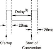
After power-up or general-call reset, the TMP102 immediately starts a conversion, as shown in Figure 11. The first result is available after 26 ms (typical). The active quiescent current during conversion is 40 μA (typical at +27°C). The quiescent current during delay is 2.2 μA (typical at +27°C).
