SBOS397H August 2007 – December 2018 TMP102
PRODUCTION DATA.
- 1 Features
- 2 Applications
- 3 Description
- 4 Revision History
- 5 Pin Configuration and Functions
- 6 Specifications
-
7 Detailed Description
- 7.1 Overview
- 7.2 Functional Block Diagram
- 7.3 Feature Description
- 7.4 Device Functional Modes
- 7.5
Programming
- 7.5.1 Pointer Register
- 7.5.2 Temperature Register
- 7.5.3
Configuration Register
- Table 10. Byte 1 of Configuration and Power-Up or Reset Format
- Table 11. Byte 2 of Configuration and Power-Up or Reset Format
- 7.5.3.1 Shutdown Mode (SD)
- 7.5.3.2 Thermostat Mode (TM)
- 7.5.3.3 Polarity (POL)
- 7.5.3.4 Fault Queue (F1/F0)
- 7.5.3.5 Converter Resolution (R1/R0)
- 7.5.3.6 One-Shot (OS)
- 7.5.3.7 EM Bit
- 7.5.3.8 Alert (AL Bit)
- 7.5.3.9 Conversion Rate (CR)
- 7.5.4 High- and Low-Limit Registers
- 8 Application and Implementation
- 9 Power Supply Recommendations
- 10Layout
- 11Device and Documentation Support
- 12Mechanical, Packaging, and Orderable Information
Package Options
Mechanical Data (Package|Pins)
- DRL|6
Thermal pad, mechanical data (Package|Pins)
Orderable Information
7.3.11 Timing Diagrams
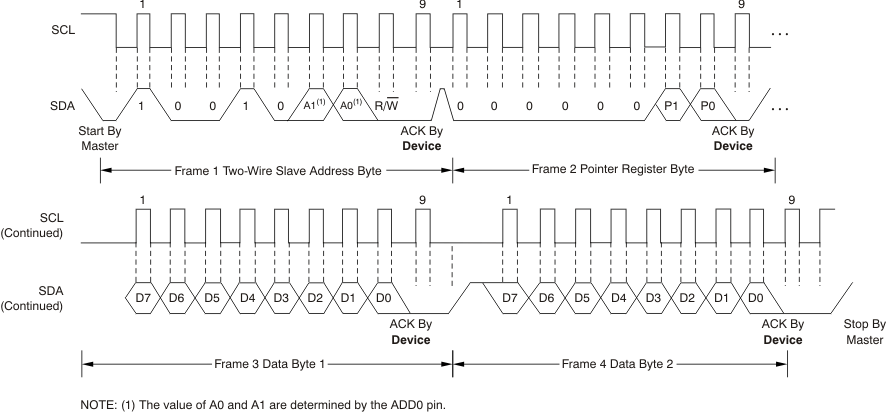
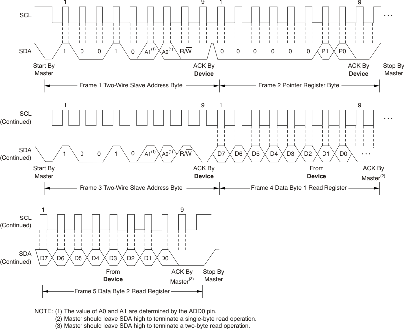
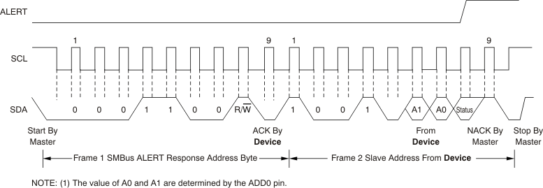
The TMP102 device is two-wire, SMBus, and I2C-interface compatible. Figure 7, Figure 8, Figure 9, and Figure 10 list the various operations on the TMP102 device. Parameters for Figure 7 are defined in the Timing Requirements table. The bus definitions are defined as follows:
- Acknowledge Each receiving device, when addressed, is obliged to generate an acknowledge bit. A device that acknowledges must pull down the SDA line during the acknowledge clock pulse in such a way that the SDA line is stable low during the high period of the Acknowledge clock pulse. Setup and hold times must be taken into account. On a master receive, the termination of the data transfer can be signaled by the master generating a not-acknowledge (1) on the last byte that has been transmitted by the slave.
- Bus Idle Both SDA and SCL lines remain high.
- Data Transfer The number of data bytes transferred between a START and a STOP condition is not limited and is determined by the master device. The TMP102 device can also be used for single byte updates. To update only the MS byte, terminate the communication by issuing a START or STOP communication on the bus.
- Start Data Transfer A change in the state of the SDA line, from high to low, when the SCL line is high, defines a START condition. Each data transfer is initiated with a START condition.
- Stop Data Transfer A change in the state of the SDA line from low to high when the SCL line is high defines a STOP condition. Each data transfer is terminated with a repeated START or STOP condition.
 Figure 7. Two-Wire Timing Diagram
  Figure 8. Two-Wire Timing Diagram for Write Word Format
  Figure 9. Two-Wire Timing Diagram for Read Word Format
  Figure 10. Timing Diagram for SMBus Alert