SLOS887F September   2014  – June 2022 TMP112-Q1

PRODUCTION DATA  

  1. Features
  2. Applications
  3. Description
  4. Revision History
  5. Description (continued)
  6. Pin Configuration and Functions
  7. Specifications
    1. 7.1 Absolute Maximum Ratings
    2. 7.2 ESD Ratings
    3. 7.3 Recommended Operating Conditions
    4. 7.4 Thermal Information
    5. 7.5 Electrical Characteristics
    6. 7.6 Specifications for User-Calibrated Systems
    7. 7.7 Timing Requirements
    8. 7.8 Typical Characteristics
  8. Detailed Description
    1. 8.1 Overview
    2. 8.2 Functional Block Diagram
    3. 8.3 Feature Description
      1. 8.3.1 Digital Temperature Output
      2. 8.3.2 Serial Interface
        1. 8.3.2.1 Bus Overview
        2. 8.3.2.2 Serial Bus Address
        3. 8.3.2.3 Writing and Reading Operation
        4. 8.3.2.4 Target Mode Operation
          1. 8.3.2.4.1 Target Receiver Mode
          2. 8.3.2.4.2 Target Transmitter Mode
        5. 8.3.2.5 SMBus Alert Function
        6. 8.3.2.6 General Call
        7. 8.3.2.7 High-Speed (Hs) Mode
        8. 8.3.2.8 Timeout Function
        9. 8.3.2.9 Timing Diagrams
          1. 8.3.2.9.1 Two-Wire Timing Diagrams
    4. 8.4 Device Functional Modes
      1. 8.4.1 Continuous-Conversion Mode
      2. 8.4.2 Extended Mode (EM)
      3. 8.4.3 Shutdown Mode (SD)
      4. 8.4.4 One-Shot and Conversion Ready Mode (OS)
      5. 8.4.5 Thermostat Mode (TM)
        1. 8.4.5.1 Comparator Mode (TM = 0)
        2. 8.4.5.2 Interrupt Mode (TM = 1)
    5. 8.5 Programming
      1. 8.5.1 Pointer Register
      2. 8.5.2 Temperature Register
      3. 8.5.3 Configuration Register
        1. 8.5.3.1 Shutdown Mode (SD)
        2. 8.5.3.2 Thermostat Mode (TM)
        3. 8.5.3.3 Polarity (POL)
        4. 8.5.3.4 Fault Queue (F1/F0)
        5. 8.5.3.5 Converter Resolution (R1 and R0)
        6. 8.5.3.6 One-Shot (OS)
        7. 8.5.3.7 Extended Mode (EM)
        8. 8.5.3.8 Alert (AL)
        9. 8.5.3.9 Conversion Rate (CR)
      4. 8.5.4 High- and Low-Limit Registers
  9. Application and Implementation
    1. 9.1 Application Information
      1. 9.1.1 Calibrating for Improved Accuracy
        1. 9.1.1.1 Example 1: Finding Worst-Case Accuracy From –15°C to 50°C
        2. 9.1.1.2 Example 2: Finding Worst-Case Accuracy From 25°C to 100°C
      2. 9.1.2 Using The Slope Specifications With a 1-Point Calibration
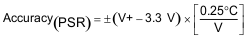
        1. 9.1.2.1 Power Supply-Level Contribution to Accuracy
    2. 9.2 Typical Application
      1. 9.2.1 Design Requirements
      2. 9.2.2 Detailed Design Procedure
      3. 9.2.3 Application Curve
  10. 10Power Supply Recommendations
  11. 11Layout
    1. 11.1 Layout Guidelines
    2. 11.2 Layout Example
  12. 12Device and Documentation Support
    1. 12.1 Documentation Support
      1. 12.1.1 Related Documentation
    2. 12.2 Receiving Notification of Documentation Updates
    3. 12.3 Community Resources
    4. 12.4 Trademarks
  13. 13Mechanical, Packaging, and Orderable Information

Package Options

Mechanical Data (Package|Pins)
Thermal pad, mechanical data (Package|Pins)
Orderable Information

Power Supply-Level Contribution to Accuracy

The superior accuracy that can be achieved with the TMP112-Q1 device is complemented by the immunity-to-DC variations from a 3.3-V supply voltage. This immunity is important because it spares the user from having to use another LDO regulator to produce 3.3 V to achieve accuracy. Nevertheless, the noise quantization that results from changing supply can add some slight change in temperature measurement accuracy. As an example, if the user chooses to operate the device at 1.8 V, the worst-case expected change in accuracy can be calculated with Equation 14:

Equation 14. GUID-91D369B6-A02A-45D3-8A6A-1C6AE2A5180A-low.gif
Equation 15. GUID-E7DB2886-99E1-4B40-86E3-475311968090-low.gif

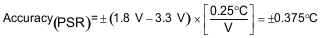
This example is a worst-case accuracy contribution as a result of variation in power supply that must be added to the accuracy plus the slope maximum.