SNIS214E june   2021  – july 2023 TMP114

PRODUCTION DATA  

  1.   1
  2. Features
  3. Applications
  4. Description
  5. Revision History
  6. Device Comparison
  7. Pin Configuration and Functions
  8. Specifications
    1. 7.1 Absolute Maximum Ratings
    2. 7.2 ESD Ratings
    3. 7.3 Recommended Operating Conditions
    4. 7.4 Thermal Information
    5. 7.5 Electrical Characteristics
    6. 7.6 I2C Interface Timing
    7. 7.7 Typical Characteristics
  9. Detailed Description
    1. 8.1 Overview
    2. 8.2 Functional Block Diagram
    3. 8.3 Feature Description
      1. 8.3.1 1.2 V Compatible Logic Inputs
      2. 8.3.2 Cyclic Redundancy Check (CRC)
      3. 8.3.3 Temperature Limits
      4. 8.3.4 Slew Rate Warning
      5. 8.3.5 NIST Traceability
    4. 8.4 Device Functional Modes
      1. 8.4.1 Continuous Conversion Mode
      2. 8.4.2 Shutdown Mode
        1. 8.4.2.1 One-Shot Temperature Conversions
    5. 8.5 Programming
      1. 8.5.1 Temperature Data Format
      2. 8.5.2 I2C and SMBus Interface
      3. 8.5.3 Device Address
      4. 8.5.4 Bus Transactions
        1. 8.5.4.1 Auto-Increment
        2. 8.5.4.2 Writes
          1. 8.5.4.2.1 CRC Enabled Writes
        3. 8.5.4.3 Reads
          1. 8.5.4.3.1 CRC Enabled Reads
        4. 8.5.4.4 General Call Reset Function
        5. 8.5.4.5 Time-Out Function
        6. 8.5.4.6 Coexist on I3C MixedBus
        7. 8.5.4.7 Cyclic Redundancy Check Implementation
    6. 8.6 Register Map
  10. Application and Implementation
    1. 9.1 Application Information
    2. 9.2 Separate I2C Pullup and Supply Application
      1. 9.2.1 Design Requirements
      2. 9.2.2 Detailed Design Procedure
      3. 9.2.3 Application Curves
    3. 9.3 Equal I2C Pullup and Supply Voltage Application
      1. 9.3.1 Design Requirements
      2. 9.3.2 Detailed Design Procedure
    4. 9.4 Power Supply Recommendations
    5. 9.5 Layout
      1. 9.5.1 Layout Guidelines
      2. 9.5.2 Layout Example
  11. 10Device and Documentation Support
    1. 10.1 Receiving Notification of Documentation Updates
    2. 10.2 Support Resources
    3. 10.3 Trademarks
    4. 10.4 Electrostatic Discharge Caution
    5. 10.5 Glossary
  12. 11Mechanical, Packaging, and Orderable Information

Package Options

Refer to the PDF data sheet for device specific package drawings

Mechanical Data (Package|Pins)
  • YMT|4
Thermal pad, mechanical data (Package|Pins)
Orderable Information

Temperature Limits

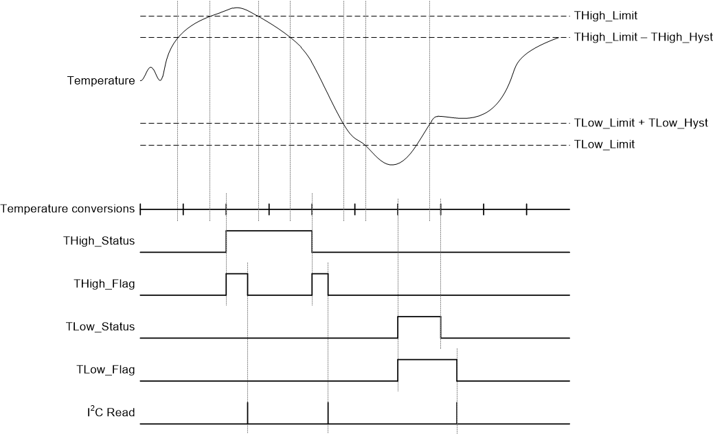
TMP114 includes an on-board temperature limit warning. At the end of every completed conversion, the TMP114 compares the result against the limits stored in the low limit register and the high limit register. When the results exceed the THigh_Limit register value, the THigh_Status and THigh_Flag bits are set. Upon read, the THigh_Flag will clear but the THigh_Status bit will remain set. After the measured temperature crosses below the THigh_Limit - THigh_Hyst value, the THigh_Status bit will clear and the THigh_Flag bit is set again to indicate a change in the temperature with respect to the limits.

If the controller is unable to read the Temp_Result register for a prolonged period of time, the flag bits can be used to determine if a thermal limit was crossed during that time. The flag bits will only clear after a successful Alert_Status register read, therefore the high and low flags can help determine if the system crossed the thermal limit before an I2C read could be performed. The Status bits will automatically update with changing Temp_Result values. Figure 8-1 depicts this behavior.
GUID-20200531-SS0I-ZVFP-MLNG-LQ8B7LWR9W9B-low.gifFigure 8-1 Alert Status Timing Diagram