SNIS214E june   2021  – july 2023 TMP114

PRODUCTION DATA  

  1.   1
  2. Features
  3. Applications
  4. Description
  5. Revision History
  6. Device Comparison
  7. Pin Configuration and Functions
  8. Specifications
    1. 7.1 Absolute Maximum Ratings
    2. 7.2 ESD Ratings
    3. 7.3 Recommended Operating Conditions
    4. 7.4 Thermal Information
    5. 7.5 Electrical Characteristics
    6. 7.6 I2C Interface Timing
    7. 7.7 Typical Characteristics
  9. Detailed Description
    1. 8.1 Overview
    2. 8.2 Functional Block Diagram
    3. 8.3 Feature Description
      1. 8.3.1 1.2 V Compatible Logic Inputs
      2. 8.3.2 Cyclic Redundancy Check (CRC)
      3. 8.3.3 Temperature Limits
      4. 8.3.4 Slew Rate Warning
      5. 8.3.5 NIST Traceability
    4. 8.4 Device Functional Modes
      1. 8.4.1 Continuous Conversion Mode
      2. 8.4.2 Shutdown Mode
        1. 8.4.2.1 One-Shot Temperature Conversions
    5. 8.5 Programming
      1. 8.5.1 Temperature Data Format
      2. 8.5.2 I2C and SMBus Interface
      3. 8.5.3 Device Address
      4. 8.5.4 Bus Transactions
        1. 8.5.4.1 Auto-Increment
        2. 8.5.4.2 Writes
          1. 8.5.4.2.1 CRC Enabled Writes
        3. 8.5.4.3 Reads
          1. 8.5.4.3.1 CRC Enabled Reads
        4. 8.5.4.4 General Call Reset Function
        5. 8.5.4.5 Time-Out Function
        6. 8.5.4.6 Coexist on I3C MixedBus
        7. 8.5.4.7 Cyclic Redundancy Check Implementation
    6. 8.6 Register Map
  10. Application and Implementation
    1. 9.1 Application Information
    2. 9.2 Separate I2C Pullup and Supply Application
      1. 9.2.1 Design Requirements
      2. 9.2.2 Detailed Design Procedure
      3. 9.2.3 Application Curves
    3. 9.3 Equal I2C Pullup and Supply Voltage Application
      1. 9.3.1 Design Requirements
      2. 9.3.2 Detailed Design Procedure
    4. 9.4 Power Supply Recommendations
    5. 9.5 Layout
      1. 9.5.1 Layout Guidelines
      2. 9.5.2 Layout Example
  11. 10Device and Documentation Support
    1. 10.1 Receiving Notification of Documentation Updates
    2. 10.2 Support Resources
    3. 10.3 Trademarks
    4. 10.4 Electrostatic Discharge Caution
    5. 10.5 Glossary
  12. 11Mechanical, Packaging, and Orderable Information

Package Options

Refer to the PDF data sheet for device specific package drawings

Mechanical Data (Package|Pins)
  • YMT|4
Thermal pad, mechanical data (Package|Pins)
Orderable Information

One-Shot Temperature Conversions

When the OS bit is set to 1b in the Configuration register, the TMP114 immediately start a one-shot temperature conversion. If the TMP114 is performing a temperature conversion, the device will stop the active conversion and discard the partial result, then start a new one-shot conversion. After completing the one-shot conversion the TMP114 will enter shutdown mode, the OS bit will be cleared, and the Mode bit will be set to 1b. If a one-shot conversion is triggered in continuous mode the device will enter shutdown mode after the one-shot conversion completes.
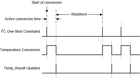
GUID-20200601-SS0I-0QPH-C9VT-KQC54RDQV7XJ-low.gif Figure 8-5 One-Shot Timing Diagram

If the One_Shot bit is continuously written as faster than the active conversion time of the TMP114, the device will continue to restart the temperature conversion with each new write to the One_Shot bit. TI recommends to avoid this behavior because the temperature result does not update until a conversion finishes. If the system triggers several continuous one-shot conversions, Figure 8-6 depicts how the device would continually partially finish new conversions and not update the Temp_Result register.
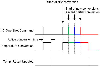
GUID-20200601-SS0I-F2MS-5MLW-4PMX1SJWZXNJ-low.gif Figure 8-6 One-Shot Continuous Trigger Timing Diagram