SNOSD82D June 2018 – September 2022 TMP117
PRODUCTION DATA
- 1 Features
- 2 Applications
- 3 Description
- 4 Revision History
- 5 Pin Configuration and Functions
- 6 Specifications
-
7 Detailed Description
- 7.1 Overview
- 7.2 Functional Block Diagrams
- 7.3 Feature Description
- 7.4 Device Functional Modes
- 7.5
Programming
- 7.5.1 EEPROM Programming
- 7.5.2 Pointer Register
- 7.5.3 I2C and SMBus Interface
- 7.6 Register Map
- 8 Application and Implementation
- 9 Power Supply Recommendations
- 10Layout
- 11Device and Documentation Support
- 12Mechanical, Packaging, and Orderable Information
Package Options
Refer to the PDF data sheet for device specific package drawings
Mechanical Data (Package|Pins)
- DRV|6
- YBG|6
Thermal pad, mechanical data (Package|Pins)
Orderable Information
7.3.2 Averaging
Users can configure the device to report the average of multiple temperature conversions with the AVG[1:0] bits to reduce noise in the conversion results. When the TMP117 is configured to perform averaging with AVG set to 01, the device executes the configured number of conversions to eight. The device accumulates those conversion results and reports the average of all the collected results at the end of the process. As shown in the noise histograms of Figure 6-6 and Figure 6-7, the temperature result output has a repeatability of approximately ±3 LSBs when there is no averaging and ±1 LSB when the device is configured to perform eight averages.
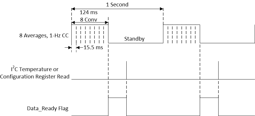
Figure 7-2 shows the total conversion cycle time trade-off when using the averaging mode to achieve this improvement in noise performance. Averaging will increase the average active current consumption due to increasing the active conversion time in a conversion cycle. For example a single active conversion typically takes 15.5 ms, so if the device is configured to report an average of eight conversions, then the active conversion time is 124 ms (15.5 ms × 8). Use Equation 1 to factor in this increase in active conversion time to accurately calculate the average current consumption of the device. The average current consumption of the device can be decreased by increasing the amount of time the device spends in standby period as compared to active conversion. Under the factory EEPROM settings, the device is configured to report an average of eight conversions with a conversion cycle time of 1 second by default.
Averaging can be used in both the continuous conversion mode and the one-shot mode.
 Figure 7-2 Averaging Timing Diagram