SNIS217C december 2020 – may 2023 TMP139
PRODUCTION DATA
- 1 Features
- 2 Applications
- 3 Description
- 4 Revision History
- 5 Pin Configuration and Functions
- 6 Specifications
-
7 Detailed Description
- 7.1 Overview
- 7.2 Functional Block Diagram
- 7.3 Feature Description
- 7.4 Device Functional Modes
- 7.5 Programming
- 7.6 Register Map
- 8 Application and Implementation
- 9 Device and Documentation Support
- 10Mechanical, Packaging, and Orderable Information
Package Options
Refer to the PDF data sheet for device specific package drawings
Mechanical Data (Package|Pins)
- YAH|6
Thermal pad, mechanical data (Package|Pins)
Orderable Information
7.4.6.8 DEVCTRL CCC
The DEVCTRL CCC is issued by the host controller for enable or disable operations that are common to devices on the bus and TMP139 shall recognize the DEVCTRL CCC.
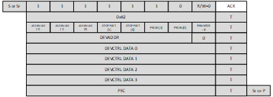
The command is generally issued in broadcast mode, but may be issued as unicast or multicast mode as well. The host may issue the DEVCTRL CCC as a generic access with RegMod field set as 0 or for a specific register access with RegMod set as 1. When RegMod field is set to 0, Figure 7-41 shows the DEVCTRL CCC packet structure when PEC is disabled. Figure 7-42 shows the structure of the DEVCTRL CCC when RegMod field is set to 0 and PEC is enabled. In the latter case the host controller shall append the PEC byte calculated on all bytes except the byte with 7'h7E and R/W=0 after the Start or Repeated Start.
 Figure 7-41 DEVCTRL CCC With REGMOD = 0 and PEC
Disabled
 Figure 7-42 DEVCTRL CCC With REGMOD = 0 and PEC
Enabled
Figure 7-42 DEVCTRL CCC With REGMOD = 0 and PEC
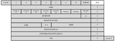
EnabledWhen RegMod field is set to 1, Figure 7-43 shows the DEVCTRL CCC packet structure when PEC is disabled. Figure 7-44 shows the structure of the DEVCTRL CCC when RegMod field is set to 1 and PEC is enabled. In the latter case the host controller shall append the PEC byte calculated on all bytes except the byte with 7'h7E and R/W = 0 after the Start or Repeated Start. If the CMD field indicates that there is only one byte to write, then the optional register data must not be sent by the host.
 Figure 7-43 DEVCTRL CCC With REGMOD = 1 and PEC
Disabled.
  Figure 7-44 DEVCTRL CCC With REGMOD = 1 and PEC
Enabled
Figure 7-44 DEVCTRL CCC With REGMOD = 1 and PEC
EnabledTMP139 NACKs the DEVCTRL CCC if the previous transaction has a parity or PEC error and the host starts the transaction with a Repeated Start.
| Field | Description | Values | Action |
|---|---|---|---|
| ADDRMASK[2:0] | Broadcast, multicast or unicast selection | 000 = Unicast command | TMP139 matches the DEVADDR[6:0] field with its serial address . |
| 011 = Multicast command | TMP139 matches the DEVADDR[6:3] field with its LID code in the serial address. | ||
| 111 = Broadcast command | TMP139 ignores the DEVADDR[6:0] and performs the required action. | ||
| STOFFSET[1:0] | Start offset byte | 00 = Byte 0 | TMP139 identifies which byte is the first byte out of DEVCTRL DATA 0, DEVCTRL DATA 1, DEVCTRL DATA 2 and DEVCTRL DATA 3 and updates its register accordingly. This field is valid only when REGMOD = 0. |
| 01 = Byte 1 | |||
| 10 = Byte 2 | |||
| 11 = Byte 3 | |||
| PECBL[1:0] | Identifies the burst length for PEC byte position | 00 = 1 Byte | TMP139 identifies the position of the PEC byte after the DEVCTRL DATA bytes are sent. This field is valid only when REGMOD = 0 and PEC is enabled. |
| 01 = 2 Byte | |||
| 10 = 3 Byte | |||
| 11 = 4 Byte | |||
| REGMOD | Identifies if it is a generic or specific register access | 0 = Generic Access | TMP139 understand the DEVCTRL DATA byte as generic data bytes described in Table 7-9 |
| 1 = Register Access | TMP139 understand the DEVCTRL DATA byte as specific register access bytes. If PEC is disabled, the format used for specific register access is as per Figure 7-11. If PEC is enabled, the format used for specific register access is as per Figure 7-13 |
| DEVCTRL DATA Bit | Function | Values | Action |
|---|---|---|---|
| DEVCTRL DATA 0 [7] | PEC Enable | 0 = Disable | MR18 register PEC_EN bit is updated |
| 1 = Enable | |||
| DEVCTRL DATA 0 [6] | Parity Disable | 0 = Enable | MR18 register PAR_DIS bit is updated |
| 1 = Disable | |||
| DEVCTRL DATA 0 [5:0] | Reserved | Reserved | |
| DEVCTRL DATA 1 [7:4] | Reserved | Reserved | |
| DEVCTRL DATA 1 [3] | Global IBI Clear | 0 = No action | MR27 register CLR_GLOBAL bit is updated |
| 1 = Clear all events and pending IBI | |||
| DEVCTRL DATA 1 [2:0] | Reserved | Reserved | |
| DEVCTRL DATA 2 [7:0] | Reserved | Reserved | |
| DEVCTRL DATA 3 [7:0] | Reserved | Reserved |
TMP139 NACKs the DEVCTRL CCC if the previous transaction has a parity or PEC error and the host starts the transaction with a Repeated Start.