SBOS891C October 2018 – September 2023 TMP144
PRODUCTION DATA
- 1
- 1 Features
- 2 Applications
- 3 Description
- 4 Revision History
- 5 Pin Configuration and Functions
- 6 Specifications
- 7 Detailed Description
- 8 Application and Implementation
- 9 Device and Documentation Support
- 10Mechanical, Packaging, and Orderable Information
Package Options
Refer to the PDF data sheet for device specific package drawings
Mechanical Data (Package|Pins)
- YBK|4
- YFF|4
- YMT|4
Thermal pad, mechanical data (Package|Pins)
Orderable Information
7.4.5 Temperature Alert Function
The TMP144 contains a temperature alert
function that monitors the device temperature and compares the result to the values
stored in the temperature limit registers to determine if the device temperature is
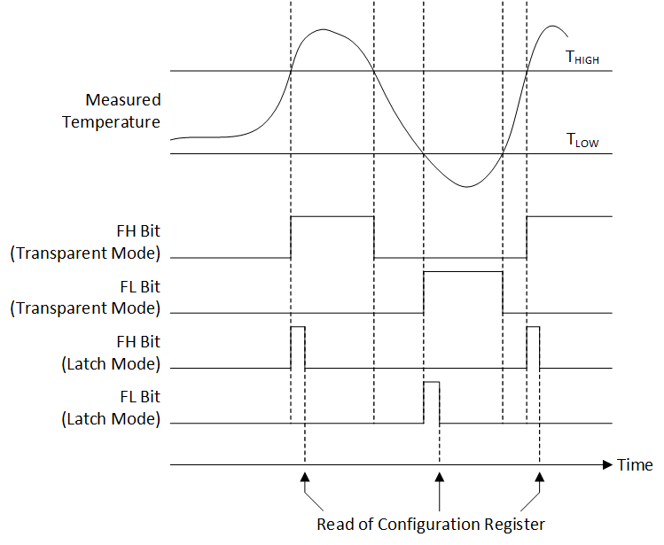
within these set limits. As shown in Figure 7-2, if the result of the temperature conversion is greater than the value in the temperature high limit register, the flag-high bit (FH) in the configuration register is set to '1'. If the result of the temperature
conversion register is less than the value in the temperature low limit register, the flag-low (FL) in the configuration
register is set to '1'. The clearing of the flag bits depends on the setting of the
latch bit (LC) in the configuration register.
 Figure 7-2 Temperature Flag Functional
Diagram.
 Figure 7-2 Temperature Flag Functional
Diagram.
 The LC bit in the configuration register when set to '1' is used to latch the value of the flag bits (FH and FL) until the host issues a read command to the configuration register. The flag bits are set to '0' when a read command is received by the device.
The LC bit when configured as '0', configures the device to operate in transparent mode, where the flag bits (FH and FL) are cleared only when the result of the temperature conversion is within the temperature limits.