SLOS889C October 2014 – September 2018 TMP302-Q1
PRODUCTION DATA.
- 1 Features
- 2 Applications
- 3 Description
- 4 Revision History
- 5 Device Comparison Table
- 6 Pin Configuration and Functions
- 7 Specifications
- 8 Detailed Description
- 9 Application and Implementation
- 10Power Supply Recommendations
- 11Layout
- 12Device and Documentation Support
- 13Mechanical, Packaging, and Orderable Information
Package Options
Mechanical Data (Package|Pins)
- DRL|6
Thermal pad, mechanical data (Package|Pins)
Orderable Information
9.2 Typical Application
Figure 10 shows the typical circuit configuration for the TMP302-Q1 family of devices. The TMP302-Q1 family of devices is configured for the default temperature threshold by connecting the TRIPSET0 and TRIPSET1 pins directly to ground. Connecting the HYSTSET pin to ground configures the device for 5°C of hysteresis. Place a 10-kΩ pullup resistor between the OUT and VS pins. Place a 0.1-µF bypass capacitor between the VS pin and ground, close to the TMP302-Q1 device.
 Figure 10. TMP302-Q1 Typical Application Schematic
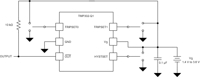
 Figure 11 shows the most generic implementation of the TMP302-Q1 family of devices. Switches are shown connecting the TMPSET0, TMPSET1 and HYSTSET pins to either VS or ground. The use of switches is not strictly required; the switches are shown only to illustrate the various pin connection combinations. In practice, connecting the TMPSET0, TMPSET1 and HYSTSET pins to ground or directly to the VS pin is sufficient and minimizes space and cost. If additional flexibility is desired, connections from the TMPSET0, TMPSET1 and HYSTSET pins can be made through 0-Ω resistors which can be either populated or not populated depending upon the desired connection.
 Figure 11. TMP302-Q1 Generic Application Schematic