SBOS876B September 2017 – February 2020 TMP461-SP
PRODUCTION DATA.
- 1 Features
- 2 Applications
- 3 Description
- 4 Revision History
- 5 Pin Configuration and Functions
- 6 Specifications
-
7 Detailed Description
- 7.1 Overview
- 7.2 Functional Block Diagram
- 7.3 Feature Description
- 7.4 Device Functional Modes
- 7.5 Programming
- 7.6
Register Map
- 7.6.1
Register Information
- 7.6.1.1 Pointer Register
- 7.6.1.2 Local and Remote Temperature Registers
- 7.6.1.3 Status Register
- 7.6.1.4 Configuration Register
- 7.6.1.5 Conversion Rate Register
- 7.6.1.6 One-Shot Start Register
- 7.6.1.7 Channel Enable Register
- 7.6.1.8 Consecutive ALERT Register
- 7.6.1.9 η-Factor Correction Register
- 7.6.1.10 Remote Temperature Offset Register
- 7.6.1.11 Manufacturer Identification Register
- 7.6.1
Register Information
- 8 Application and Implementation
- 9 Power Supply Recommendations
- 10Layout
- 11Device and Documentation Support
- 12Mechanical, Packaging, and Orderable Information
Package Options
Mechanical Data (Package|Pins)
- HKU|10
Thermal pad, mechanical data (Package|Pins)
Orderable Information
7.3.6 ALERT and THERM Functions
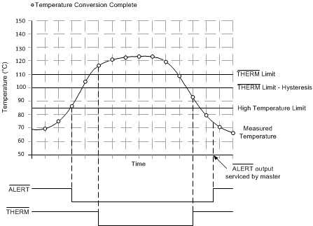
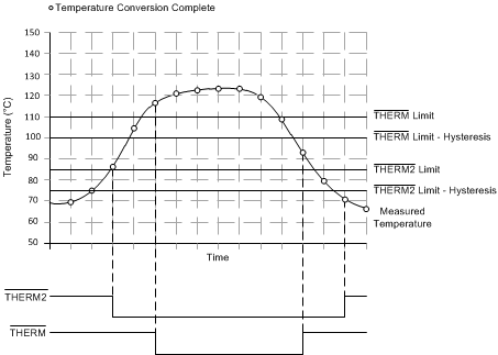
Operation of the ALERT (pin 7) and THERM (pin 4) interrupts is shown in Figure 13. Operation of the THERM (pin 4) and THERM2 (pin 7) interrupts is shown in Figure 14. The ALERT and THERM pin setting is determined by bit 5 of the configuration register.
The hysteresis value is stored in the THERM hysteresis register and applies to both the THERM and THERM2 interrupts. The value of the CONAL[2:0] bits in the consecutive ALERT register (see Table 5) determines the number of limit violations before the ALERT pin is tripped. The default value is 000b and corresponds to one violation, 001b programs two consecutive violations, 011b programs three consecutive violations, and 111b programs four consecutive violations. The CONAL[2:0] bits provide additional filtering for the ALERT pin state.

